SLVSJO5 August 2025 SN74AHCT541-Q1
PRODUCTION DATA
- 1
- 1 Features
- 2 Applications
- 3 Description
- 4 Pin Configuration and Functions
- 5 Specifications
- 6 Parameter Measurement Information
- 7 Detailed Description
- 8 Application and Implementation
- 9 Device and Documentation Support
- 10Revision History
- 11Mechanical, Packaging, and Orderable Information
Package Options
Mechanical Data (Package|Pins)
Thermal pad, mechanical data (Package|Pins)
Orderable Information
3 Description
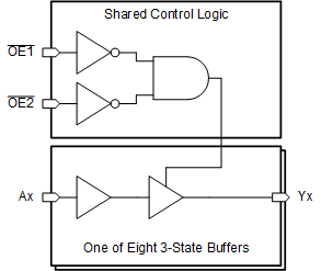
The SN74AHCT541-Q1 contains eight non-inverting buffers with 3-state outputs. The active low output enable pins (OE1 and OE2) control all eight channels, and are configured so that both must be low for the outputs to be active.
Device Information
| PART NUMBER | PACKAGE(1) | PACKAGE SIZE(2) | BODY SIZE(3) |
|---|---|---|---|
| SN74AHCT541-Q1 | PW (TSSOP, 20) | 6.5mm × 6.4mm | 6.5mm x 4.4mm |
| DGS (VSSOP, 20) | 5.1mm × 4.9mm | 5.1mm × 3.0mm | |
| RKS (VQFN, 20) | 4.5mm × 2.5mm | 4.5mm × 2.5mm |
(1) For more information, see Mechanical, Packaging, and Orderable Information.
(2) The package size (length × width)
is a nominal value and includes pins, where applicable.
(3) The body size (length × width) is
a nominal value and does not include pins.
 Functional Block Diagram