SCES576H June 2004 – March 2024 SN74AVC4T245
PRODUCTION DATA
- 1
- 1 Features
- 2 Applications
- 3 Description
- 4 Pin Configuration and Functions
-
5 Specifications
- 5.1 Absolute Maximum Ratings
- 5.2 ESD Ratings
- 5.3 Recommended Operating Conditions
- 5.4 Thermal Information
- 5.5 Electrical Characteristics
- 5.6 Operating Characteristics
- 5.7 Switching Characteristics: VCCA = 1.2V
- 5.8 Switching Characteristics: VCCA = 1.5V ± 0.1V
- 5.9 Switching Characteristics: VCCA = 1.8V ± 0.15V
- 5.10 Switching Characteristics: VCCA = 2.5V ± 0.2V
- 5.11 Switching Characteristics: VCCA = 3.3V ± 0.3V
- 5.12 Typical Characteristics
- 6 Parameter Measurement Information
- 7 Detailed Description
- 8 Application and Implementation
- 9 Device and Documentation Support
- 10Revision History
- 11Mechanical, Packaging, and Orderable Information
Package Options
Refer to the PDF data sheet for device specific package drawings
Mechanical Data (Package|Pins)
- PW|16
- RGY|16
- D|16
- DGV|16
- RSV|16
Thermal pad, mechanical data (Package|Pins)
Orderable Information
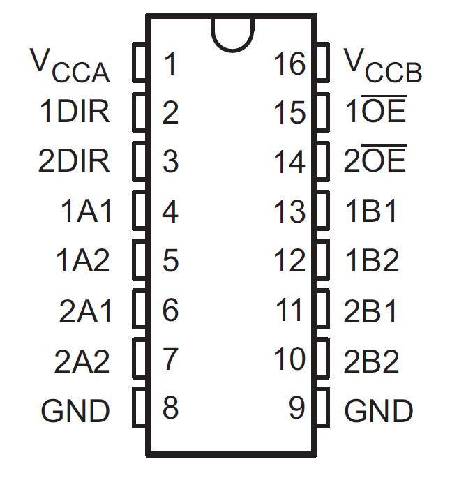
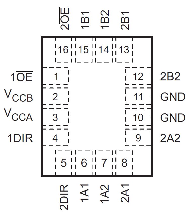
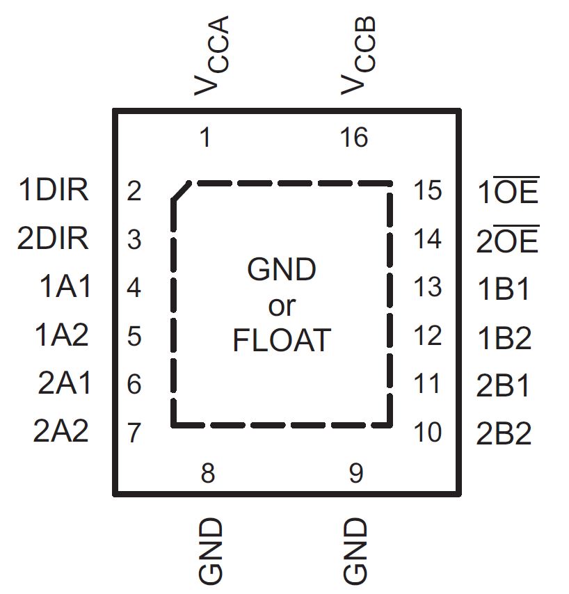
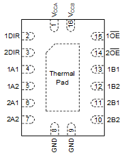
4 Pin Configuration and Functions
 Figure 4-1 D, DGV, or PW Package,
16-Pin SOIC, TVSOP, or PW (Top View)
 Figure 4-3 RSV Package, 16-Pin UQFN
(Top View)
 Figure 4-5 DYY Package, 16-Pin SOT
(Top View)
 Figure 4-2 RGY Package, 16-Pin WQFN
(Top View)
 Figure 4-4 BQB/WBQB Package, 16-Pin
WQFN (Transparent Top View)
Figure 4-4 BQB/WBQB Package, 16-Pin
WQFN (Transparent Top View)Table 4-1 Pin Functions
| PIN | NO. | TYPE(1) | DESCRIPTION | ||
|---|---|---|---|---|---|
| NAME | D, DGV, PW, RGY |
RSV | |||
| 1A1 | 4 | 6 | I/O | Input/output 1A1. Referenced to VCCA. | |
| 1A2 | 5 | 7 | I/O | Input/output 1A2. Referenced to VCCA. | |
| 1B1 | 13 | 15 | I/O | Input/output 1B1. Referenced to VCCB. | |
| 1B2 | 12 | 14 | I/O | Input/output 1B2. Referenced to VCCB. | |
| 1DIR | 2 | 4 | I | Direction-control input for ‘1’ ports | |
| 1 OE | 15 | 1 | I | 3-state output-mode enables. Pull OE high to place ‘1’ outputs in 3-state mode. Referenced to VCCA. | |
| 2A1 | 6 | 8 | I/O | Input/output 2A1. Referenced to VCCA. | |
| 2A2 | 7 | 9 | I/O | Input/output 2A2. Referenced to VCCA. | |
| 2B1 | 11 | 13 | I/O | Input/output 2B1. Referenced to VCCB. | |
| 2B2 | 10 | 12 | I/O | Input/output 2B2. Referenced to VCCB. | |
| 2DIR | 3 | 5 | I | Direction-control input for ‘2’ ports | |
| 2 OE | 14 | 16 | I | 3-state output-mode enables. Pull OE high to place ‘2’ outputs in 3-state mode. Referenced to VCCA. | |
| GND | 8, 9 | 10, 11 | — | Ground | |
| VCCA | 1 | 3 | — | A-port power supply voltage. 1.2V ≤ VCCA ≤ 3.6V | |
| VCCB | 16 | 2 | — | B-port power supply voltage. 1.2V ≤ VCCB ≤ 3.6V | |
(1) I = input, O = output