SCES901D February 2019 – January 2024 SN74AXC1T45-Q1
PRODUCTION DATA
- 1
- 1 Features
- 2 Applications
- 3 Description
- 4 Pin Configuration and Functions
- 5 Specifications
- 6 Parameter Measurement Information
-
7 Detailed Description
- 7.1 Overview
- 7.2 Functional Block Diagram
- 7.3
Feature Description
- 7.3.1 Standard CMOS Inputs
- 7.3.2 Balanced High-Drive CMOS Push-Pull Outputs
- 7.3.3 Partial Power Down (Ioff)
- 7.3.4 VCC Isolation
- 7.3.5 Over-voltage Tolerant Inputs
- 7.3.6 Negative Clamping Diodes
- 7.3.7 Fully Configurable Dual-Rail Design
- 7.3.8 I/Os with Integrated Static Pull-Down Resistors
- 7.3.9 Supports High-Speed Translation
- 7.4 Device Functional Modes
- 8 Application and Implementation
- 9 Device and Documentation Support
- 10Revision History
- 11Mechanical, Packaging, and Orderable Information
Package Options
Refer to the PDF data sheet for device specific package drawings
Mechanical Data (Package|Pins)
- DCK|6
- DRY|6
Thermal pad, mechanical data (Package|Pins)
Orderable Information
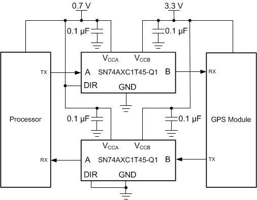
8.2.2 Universal Asynchronous Receiver-Transmitter (UART) Interface Application
Figure 8-3 shows the SN74AXC1T45-Q1 being used for the two-bit UART interface application. One SN74AXC1T45-Q1 device is used to level shift the voltage and drive the TX from the processor to the GPS Module while a second SN74AXC1T45-Q1 device is used to drive the TX Data line from the GPS Module to the Processor.
 Figure 8-3 UART Interface Application