SCES876A August 2018 – January 2019 SN74AXCH8T245
PRODUCTION DATA.
- 1 Features
- 2 Applications
- 3 Description
- 4 Revision History
- 5 Pin Configuration and Functions
-
6 Specifications
- 6.1 Absolute Maximum Ratings
- 6.2 ESD Ratings
- 6.3 Recommended Operating Conditions
- 6.4 Thermal Information
- 6.5 Electrical Characteristics
- 6.6 Switching Characteristics, VCCA = 0.7 V
- 6.7 Switching Characteristics, VCCA = 0.8 V
- 6.8 Switching Characteristics, VCCA = 0.9 V
- 6.9 Switching Characteristics, VCCA = 1.2 V
- 6.10 Switching Characteristics, VCCA = 1.5 V
- 6.11 Switching Characteristics, VCCA = 1.8 V
- 6.12 Switching Characteristics, VCCA = 2.5 V
- 6.13 Switching Characteristics, VCCA = 3.3 V
- 6.14 Operating Characteristics: TA = 25°C
- 7 Parameter Measurement Information
- 8 Detailed Description
- 9 Application and Implementation
- 10Power Supply Recommendations
- 11Layout
- 12Device and Documentation Support
- 13Mechanical, Packaging, and Orderable Information
Package Options
Mechanical Data (Package|Pins)
Thermal pad, mechanical data (Package|Pins)
Orderable Information
3 Description
The SN74AXCH8T245 device is an 8-bit non-inverting bus transceiver that resolves voltage level mismatch between devices operating at the latest voltage nodes (0.7 V, 0.8 V, and 0.9 V) and devices operating at industry standard voltage nodes (1.8 V, 2.5 V, 3.3 V) and vice versa.
The device operates by using two independent power-supply rails (VCCA and VCCB) . Data pins A1 through A8 are designed to track VCCA, which accepts any supply voltage from 0.65 V to 3.6 V. Data pins B1 through B8 are designed to track VCCB, which accepts any supply voltage from 0.65 V to 3.6 V. Additionally the SN74AXCH8T245 is compatible with a single-supply system.
The SN74AXCH8T245 device is designed for asynchronous communication between data buses. The device transmits data from the A bus to the B bus or from the B bus to the A bus, depending on the logic level of the direction-control inputs (DIR1 and DIR2). The output-enable (OE) input is used to disable the outputs so the buses are effectively isolated.
The SN74AXCH8T245 device is designed so the control pins (DIR and OE) are referenced to VCCA.
Active bus-hold circuitry holds unused or undriven inputs at a valid logic state. Use of pull-up or pull-down resistors with the bus-hold circuitry is not recommended. If a supply is present for VCCA or VCCB, the bus-hold circuitry always remains active on all A and B ports respectively, independent of the direction control or output enable.
This device is fully specified for partial-power-down applications using Ioff. The Ioff circuitry disables the outputs when the device is powered down. This inhibits current backflow into the device which prevents damage to the device.
The VCC isolation feature ensures that if either VCC input supply is below 100 mV, all level shifter outputs are disabled and placed into a high-impedance state. To ensure the high-impedance state of the level shifter I/Os during power up or power down, OE should be tied to VCCA through a pull-up resistor; the minimum value of the resistor is determined by the current-sinking capability of the driver.
Device Information(1)
| PART NUMBER | PACKAGE | BODY SIZE (NOM) |
|---|---|---|
| SN74AXCH8T245PW | TSSOP (24) | 7.80 mm × 4.40 mm |
| SN74AXCH8T245RHL | VQFN (24) | 5.50 mm × 3.50 mm |
- For all available packages, see the orderable addendum at the end of the data sheet.
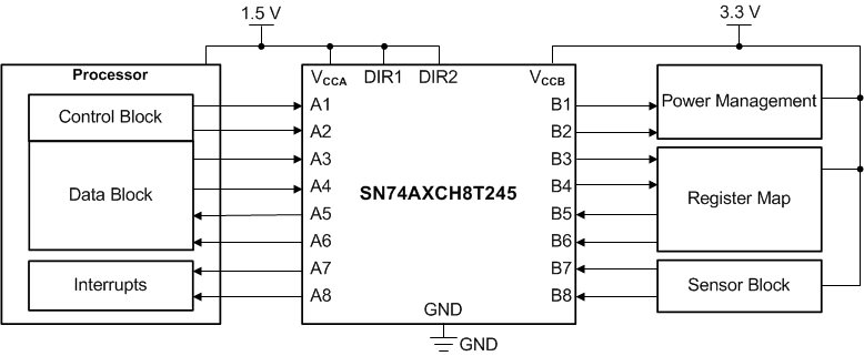
Typical Application Schematic
