SCDS120C February 2003 – December 2018 SN74CB3T3125
PRODUCTION DATA.
- 1 Features
- 2 Applications
- 3 Description
- 4 Revision History
- 5 Pin Configuration and Functions
- 6 Specifications
- 7 Parameter Measurement Information
- 8 Detailed Description
- 9 Application and Implementation
- 10Power Supply Recommendations
- 11Layout
- 12Device and Documentation Support
- 13Mechanical, Packaging, and Orderable Information
Package Options
Refer to the PDF data sheet for device specific package drawings
Mechanical Data (Package|Pins)
- RGY|14
- DGV|14
- PW|14
Thermal pad, mechanical data (Package|Pins)
- RGY|14
Orderable Information
3 Description
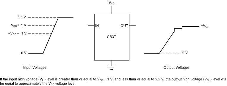
The SN74CB3T3125 is a high-speed TTL-compatible FET bus switch with low ON-state resistance (ron), allowing for minimal propagation delay. The device fully supports mixed-mode signal operation on all data I/O ports by providing voltage translation that tracks VCC. The SN74CB3T3125 supports systems using 5-V TTL, 3.3-V LVTTL, and 2.5-V CMOS switching standards, as well as user-defined switching levels (see Typical DC Voltage-Translation Characteristics).
The SN74CB3T3125 is organized as four 1-bit bus switches with separate output-enable (1OE, 2OE, 3OE, 4OE) inputs. It can be used as four 1-bit bus switches or as one 4-bit bus switch. When OE is low, the associated 1-bit bus switch is ON, and the A port is connected to the B port, allowing bidirectional data flow between ports. When OE is high, the associated 1-bit bus switch is OFF, and the high-impedance state exists between the A and B ports.
This device is fully specified for partial-power-down applications using Ioff. The Ioff feature ensures that damaging current will not backflow through the device when it is powered down. The device has isolation during power off.
To ensure the high-impedance state during power up or power down, OE should be tied to VCC through a pullup resistor; the minimum value of the resistor is determined by the current-sinking capability of the driver.
Device Information(1)
| PART NUMBER | PACKAGE | BODY SIZE (NOM) |
|---|---|---|
| SN74CB3T3125 | VQFN – RGY (14) | 3.50 mm x 3.50 mm |
| TSSOP – PW (14) | 5.00 mm x 4.40 mm | |
| TVSOP – DGV (14) | 3.60 mm x 4.40 mm |
- For all available packages, see the orderable addendum at the end of the data sheet.
