SCLS774 October 2019 SN74HCS72-Q1
PRODUCTION DATA.
- 1 Features
- 2 Applications
- 3 Description
- 4 Revision History
- 5 Pin Configuration and Functions
- 6 Specifications
- 7 Parameter Measurement Information
- 8 Detailed Description
- 9 Application and Implementation
- 10Power Supply Recommendations
- 11Layout
- 12Device and Documentation Support
- 13Mechanical, Packaging, and Orderable Information
Package Options
Mechanical Data (Package|Pins)
Thermal pad, mechanical data (Package|Pins)
Orderable Information
7 Parameter Measurement Information
Phase relationships between waveforms were chosen arbitrarily. All input pulses are supplied by generators having the following characteristics: PRR ≤ 1 MHz, ZO = 50 Ω, tt < 2.5 ns.
For clock inputs, fmax is measured when the input duty cycle is 50%.
The outputs are measured one at a time with one input transition per measurement.

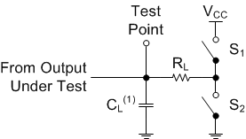
1. CL includes probe and test-fixture capacitance.
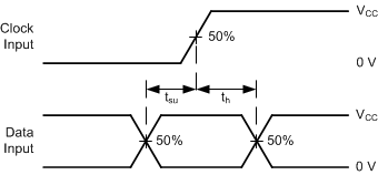
Figure 5. Load Circuit  Figure 7. Voltage Waveforms, Setup and Hold Times
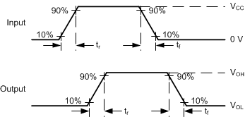
  Figure 9. Voltage Waveforms, Input and Output Transition Times
  Figure 6. Voltage Waveforms, Pulse Duration
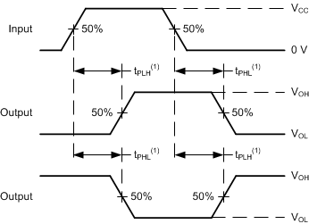
1. Voltage Waveforms, Propagation Delay specifications tPLH and tPHL are the same as tpd.
Figure 8. Voltage Waveforms Propagation Delays