SCES515M December 2003 – November 2022 SN74LVC1T45
PRODUCTION DATA
- 1 Features
- 2 Applications
- 3 Description
- 4 Revision History
- 5 Pin Configuration and Functions
-
6 Specifications
- 6.1 Absolute Maximum Ratings
- 6.2 ESD Ratings
- 6.3 Recommended Operating Conditions
- 6.4 Thermal Information
- 6.5 Electrical Characteristics
- 6.6 Switching Characteristics (VCCA = 1.8 V ± 0.15 V)
- 6.7 Switching Characteristics (VCCA = 2.5 V ± 0.2 V)
- 6.8 Switching Characteristics (VCCA = 3.3 V ± 0.3 V)
- 6.9 Switching Characteristics (VCCA = 5 V ±0.5 V)
- 6.10 Operating Characteristics
- 6.11 Typical Characteristics
- 7 Parameter Measurement Information
- 8 Detailed Description
- 9 Applications and Implementation
- 10Power Supply Recommendations
- 11Layout
- 12Device and Documentation Support
- 13Mechanical, Packaging, and Orderable Information
Package Options
Mechanical Data (Package|Pins)
Thermal pad, mechanical data (Package|Pins)
Orderable Information
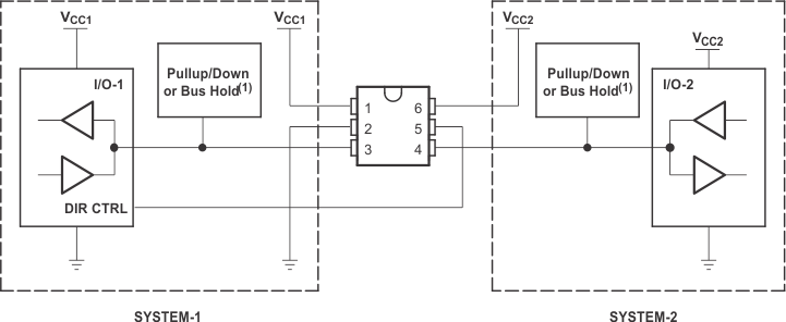
9.2.2 Bidirectional Logic Level-Shifting Application
Figure 9-3 shows the SN74LVC1T45 being used in a bidirectional logic level-shifting application. Because the SN74LVC1T45 does not have an output-enable (OE) pin, the system designer should take precautions to avoid bus contention between SYSTEM-1 and SYSTEM-2 when changing directions.
 Figure 9-3 Bidirectional Logic Level-Shifting Application