SCES515M December 2003 – November 2022 SN74LVC1T45
PRODUCTION DATA
- 1 Features
- 2 Applications
- 3 Description
- 4 Revision History
- 5 Pin Configuration and Functions
-
6 Specifications
- 6.1 Absolute Maximum Ratings
- 6.2 ESD Ratings
- 6.3 Recommended Operating Conditions
- 6.4 Thermal Information
- 6.5 Electrical Characteristics
- 6.6 Switching Characteristics (VCCA = 1.8 V ± 0.15 V)
- 6.7 Switching Characteristics (VCCA = 2.5 V ± 0.2 V)
- 6.8 Switching Characteristics (VCCA = 3.3 V ± 0.3 V)
- 6.9 Switching Characteristics (VCCA = 5 V ±0.5 V)
- 6.10 Operating Characteristics
- 6.11 Typical Characteristics
- 7 Parameter Measurement Information
- 8 Detailed Description
- 9 Applications and Implementation
- 10Power Supply Recommendations
- 11Layout
- 12Device and Documentation Support
- 13Mechanical, Packaging, and Orderable Information
Package Options
Mechanical Data (Package|Pins)
Thermal pad, mechanical data (Package|Pins)
Orderable Information
5 Pin Configuration and Functions
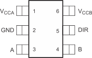
 Figure 5-1 DBV Package,6-Pin SOT-23(Top View)
 Figure 5-3 DRL Package,6-Pin SOT(Top View)
 Figure 5-2 DCK Package,6-Pin SC70(Top View)
 Figure 5-4 DPK Package,6-Pin USON(Top View)
Table 5-1 Pin Functions
| PIN | TYPE(1) | DESCRIPTION | ||
|---|---|---|---|---|
| NAME | DBV, DCK, DRL, DPK | |||
| VCCA | 1 | P | SYSTEM-1 supply voltage (1.65 V to 5.5 V) | |
| GND | 2 | G | Device GND | |
| A | 3 | I/O | Output level depends on VCC1 voltage. | |
| B | 4 | I/O | Input threshold value depends on VCC2 voltage. | |
| DIR | 5 | I | GND (low level) determines B-port to A-port direction. | |
| VCCB | 6 | P | SYSTEM-2 supply voltage (1.65 V to 5.5 V) | |
(1) P = power, G = ground, I/O = input and output, I = input
Figure 5-5 YZP Package,6-Pin DSBGA(Bottom View)
| Legend | |
|---|---|
| Power | Input |
| Input or Output | Ground |
Table 5-2 Pin Functions
| PIN | TYPE(1) | DESCRIPTION | |
|---|---|---|---|
| NO. | NAME | ||
| A1 | VCCA | P | SYSTEM-1 supply voltage (1.65 V to 5.5 V) |
| A2 | VCCB | P | SYSTEM-2 supply voltage (1.65 V to 5.5 V) |
| B1 | GND | G | Device GND |
| B2 | DIR | I | GND (low level) determines B-port to A-port direction. |
| C1 | A | I/O | Output level depends on VCC1 voltage. |
| C2 | B | I/O | Input threshold value depends on VCC2 voltage. |
(1) P = power, G = ground, I/O = input and output, I =
input