SCES557E March 2004 – October 2020 SN74LVC2G08-Q1
PRODUCTION DATA
- 1 Features
- 2 Applications
- 3 Description
- 4 Revision History
- 5 Pin Configuration and Functions
- 6 Specifications
- 7 Typical Characteristics
- 8 Parameter Measurement Information
- 9 Detailed Description
- 10Application and Implementation
- 11Application Curves
- 12Power Supply Recommendations
- 13Layout
- 14Device and Documentation Support
- 15Mechanical, Packaging, and Orderable Information
Package Options
Refer to the PDF data sheet for device specific package drawings
Mechanical Data (Package|Pins)
- DCU|8
- DCT|8
Thermal pad, mechanical data (Package|Pins)
Orderable Information
3 Description
This dual 2-input positive-AND gate is designed for 1.65-V to 5.5-V VCC operation.
The SN74LVC2G08-Q1 performs the
Boolean function 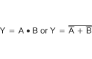 in
positive logic.
in
positive logic.
This device is fully specified for partial-power-down applications using Ioff. The Ioff circuitry disables the outputs, preventing damaging current backflow through the device when it is powered down.
Device Information(1)
| PART NUMBER | PACKAGE | BODY SIZE (NOM) |
|---|---|---|
| SN74LVC2G08DCT-Q1 | SM8 (8) | 2.95 mm × 2.80 mm |
| SN74LVC2G08DCU-Q1 | VSSOP (8) | 2.30 mm × 2.00 mm |
(1) For all available packages, see the orderable addendum at the
end of the data sheet.
") Figure 3-1 Logic Diagram (Positive
Logic)
Figure 3-1 Logic Diagram (Positive
Logic)