SLRS023E December 1976 – January 2015 SN75468 , SN75469
PRODUCTION DATA.
- 1 Features
- 2 Applications
- 3 Description
- 4 Simplified Schematic
- 5 Revision History
- 6 Pin Configuration and Functions
- 7 Specifications
- 8 Parameter Measurement Information
- 9 Detailed Description
- 10Application and Implementation
- 11Power Supply Recommendations
- 12Layout
- 13Device and Documentation Support
- 14Mechanical, Packaging, and Orderable Information
Package Options
Refer to the PDF data sheet for device specific package drawings
Mechanical Data (Package|Pins)
- N|16
- D|16
Thermal pad, mechanical data (Package|Pins)
Orderable Information
12 Layout
12.1 Layout Guidelines
Thin traces can be used on the input due to the low current logic that is typically used to drive SN75468. Care must be taken to separate the input channels as much as possible, as to eliminate cross-talk. Thick traces are recommended for the output, in order to drive whatever high currents that may be needed. Wire thickness can be determined by the trace material's current density and desired drive current.
Since all of the channels currents return to a common emitter, it is best to size that trace width to be very wide. Some applications require up to 2.5 A.
12.2 Layout Example
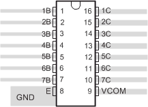 Figure 22. Package Layout