SLRS023E December 1976 – January 2015 SN75468 , SN75469
PRODUCTION DATA.
- 1 Features
- 2 Applications
- 3 Description
- 4 Simplified Schematic
- 5 Revision History
- 6 Pin Configuration and Functions
- 7 Specifications
- 8 Parameter Measurement Information
- 9 Detailed Description
- 10Application and Implementation
- 11Power Supply Recommendations
- 12Layout
- 13Device and Documentation Support
- 14Mechanical, Packaging, and Orderable Information
Package Options
Refer to the PDF data sheet for device specific package drawings
Mechanical Data (Package|Pins)
- N|16
- D|16
Thermal pad, mechanical data (Package|Pins)
Orderable Information
7 Specifications
7.1 Absolute Maximum Ratings
over operating free-air temperature range (unless otherwise noted)(1)| MIN | MAX | UNIT | |||
|---|---|---|---|---|---|
| VCE | Collector-emitter voltage | 100 | V | ||
| VI | Input voltage(2) | 30 | V | ||
| Peak collector current | 500 | mA | |||
| IOK | Output clamp current | 500 | mA | ||
| Total emitter-terminal current | –2.5 | A | |||
| TJ | Operating virtual junction temperature | 150 | °C | ||
| Tstg | Storage temperature range | –65 | 150 | °C | |
(1) Stresses beyond those listed under Absolute Maximum Ratings may cause permanent damage to the device. These are stress ratings only, which do not imply functional operation of the device at these or any other conditions beyond those indicated under Recommended Operating Conditions. Exposure to absolute-maximum-rated conditions for extended periods may affect device reliability.
(2) All voltage values are with respect to the emitter/substrate terminal E, unless otherwise noted.
7.2 ESD Ratings
| VALUE | UNIT | |||
|---|---|---|---|---|
| V(ESD) | Electrostatic discharge | Human body model (HBM), per ANSI/ESDA/JEDEC JS-001, all pins(1) | ±2000 | V |
| Charged device model (CDM), per JEDEC specification JESD22-C101, all pins(2) | ±500 | |||
(1) JEDEC document JEP155 states that 500-V HBM allows safe manufacturing with a standard ESD control process.
(2) JEDEC document JEP157 states that 250-V CDM allows safe manufacturing with a standard ESD control process.
7.3 Recommended Operating Conditions
over operating free-air temperature range (unless otherwise noted)| MIN | MAX | UNIT | ||
|---|---|---|---|---|
| VI | 0 | 5 | V | |
| VCC | 0 | 100 | V | |
| TJ | Junction Temperature | –40 | 125 | °C |
7.4 Thermal Information
| THERMAL METRIC(1) | SN7546x | UNIT | |
|---|---|---|---|
| D | |||
| 16 PINS | |||
| RθJA | Junction-to-ambient thermal resistance | 73 | °C/W |
| RθJC(top) | Junction-to-case (top) thermal resistance | 40.3 | |
| RθJB | Junction-to-board thermal resistance | 38.9 | |
| ψJT | Junction-to-top characterization parameter | 10.9 | |
| ψJB | Junction-to-board characterization parameter | 38.7 | |
| RθJC(bot) | Junction-to-case (bottom) thermal resistance | N/A | |
(1) For more information about traditional and new thermal metrics, see the IC Package Thermal Metrics application report, SPRA953.
7.5 Electrical Characteristics
TA = 25°C (unless otherwise noted)| PARAMETER | TEST CONDITIONS(1) | SN75468 | SN75469 | UNIT | ||||||||
|---|---|---|---|---|---|---|---|---|---|---|---|---|
| MIN | TYP | MAX | MIN | TYP | MAX | |||||||
| VI(on) | On-state input voltage | VCE = 2 V | IC = 125 mA | V | ||||||||
| IC = 200 mA | 2.4 | |||||||||||
| IC = 250 mA | 2.7 | |||||||||||
| IC = 275 mA | ||||||||||||
| IC = 300 mA | 3 | |||||||||||
| IC = 350 mA | ||||||||||||
| VCE(sat) | Collector-emitter saturation voltage | II = 250 µA, IC = 100 mA | 0.9 | 1.1 | 0.9 | 1.1 | V | |||||
| II = 350 µA, IC = 100 mA | 1 | 1.3 | 1 | 1.3 | ||||||||
| II = 500 µA, IC = 100 mA | 1.2 | 1.6 | 1.2 | 1.6 | ||||||||
| VF | Clamp-diode forward voltage | IF = 350 mA | 1.7 | 2 | 1.7 | 2 | V | |||||
| ICEX | collector cutoff current | VCE = 100 V, II = 0 | 50 | 50 | µA | |||||||
| VCE = 100 V, TA = 70°C |
II = 0 | 100 | 100 | |||||||||
| VI = 1 V | 500 | |||||||||||
| II(off) | Off-state input current | VCE = 50 V, IC = 500 µA, TA = 70°C | 50 | 65 | 50 | 65 | µA | |||||
| II | Input current | VI = 3.85 V | 0.93 | 1.35 | mA | |||||||
| VI = 5 V | 0.35 | 0.5 | ||||||||||
| VI = 12 V | 1 | 1.45 | ||||||||||
| IR | Clamp-diode reverse current | VR = 100 V | 50 | 50 | µA | |||||||
| VR = 100 V, TA = 70°C | 100 | 10 | ||||||||||
| Ci | Input Capacitance | VI = 0, f = 1 MHz | 15 | 25 | 15 | 25 | pF | |||||
(1) All electrical characteristics are measured with 0.1-µF capacitors connected at REF, CT, and VCC to GND.
7.6 Switching Characteristics
TA = 25°C free-air temperature| PARAMETER | TEST CONDITIONS(1) | MIN | TYP | MAX | UNIT | ||
|---|---|---|---|---|---|---|---|
| tPLH | Propagation delay time, low-to-high-level output | VS = 20 V, RL = 163 Ω, CL = 15 pF, See Figure 14 | 0.25 | 1 | µs | ||
| tPHL | Propagation delay time, high-to-low-level output | 0.25 | 1 | µs | |||
| VOH | High-level output voltage after switching | VS = 50 V, IO = 300 mA, See Figure 14 | VS – 20 | mV | |||
(1) All switching characteristics are measured with 0.1-µF capacitors connected at REF and VCC to GND.
7.7 Typical Characteristics
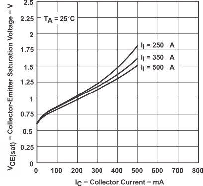 Figure 1. Collector-Emitter Saturation Voltage
vs
Collector Current (One Darlington)
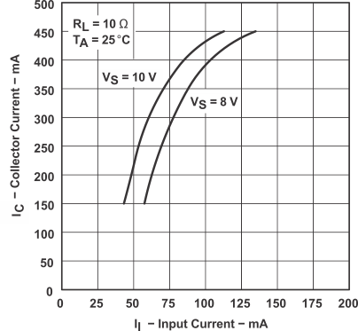 Figure 3. Output Current vs Input Current
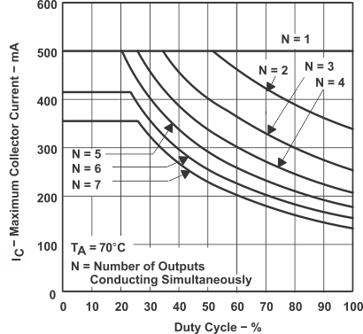 Figure 5. N Package Maximum Collector Current
vs
Duty Cycle
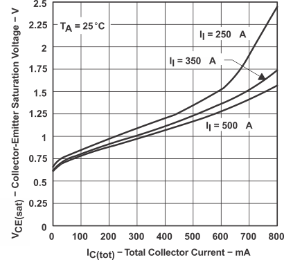 Figure 2. Collector-Emitter Saturation Voltage
vs
Total Collector Current (Two Darlingtons in Parallel)
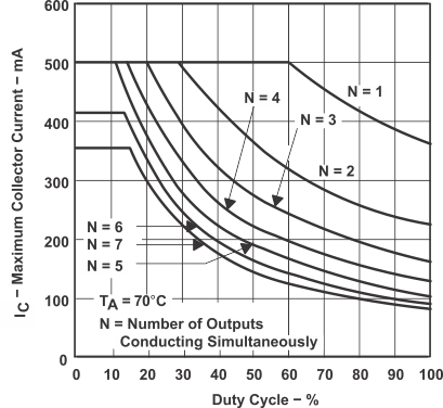 Figure 4. D Package Maximum Collector Current
vs
Duty Cycle