SLLS121E August 1990 – April 2024 SN75ALS172A
PRODUCTION DATA
- 1
- 1 Feature
- 2 Applications
- 3 Description
- 4 Pin Configuration and Functions
- 5 Specifications
- 6 Parameter Measurement Information
- 7 Detailed Description
- 8 Device and Documentation Support
- 9 Revision History
- 10Mechanical, Packaging, and Orderable Information
Package Options
Refer to the PDF data sheet for device specific package drawings
Mechanical Data (Package|Pins)
- N|16
- DW|20
Thermal pad, mechanical data (Package|Pins)
Orderable Information
3 Description
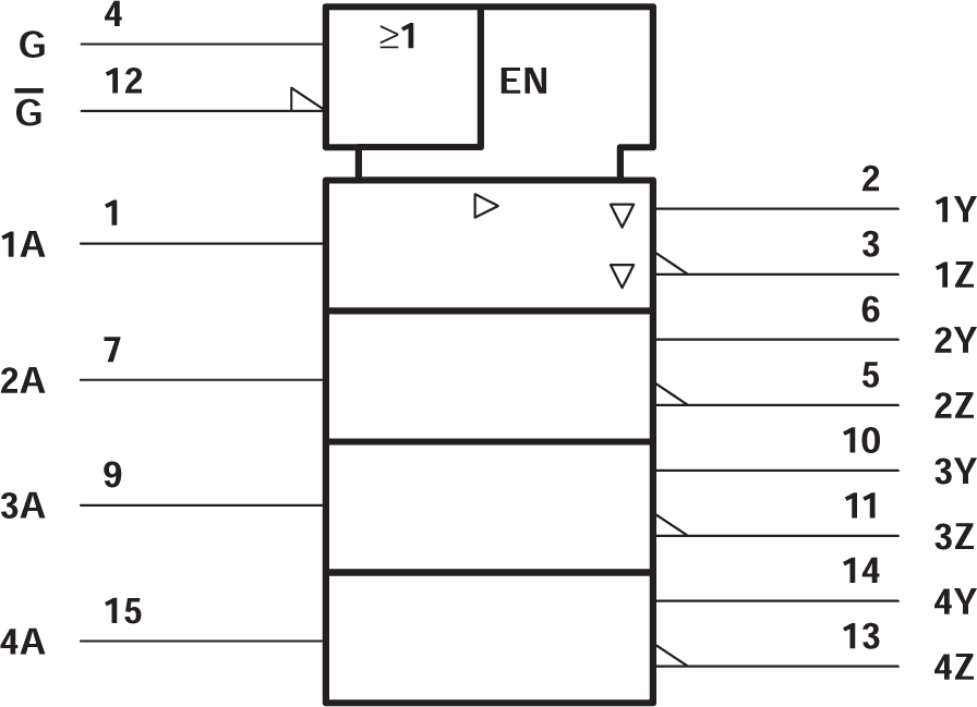
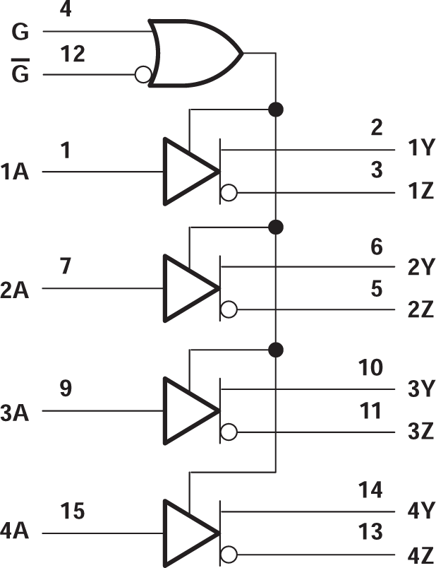
The SN75ALS172A comprises four line drivers with 3-state differential outputs. Which are designed to meet the requirements of ANSI Standards EIA/TIA-422-B and RS-485 and ITU Recommendation V.11. The device is optimized for balanced multipoint bus transmission at rates of up to 20Mbaud. Each driver features wide positive and negative common-mode output voltage ranges, making the driver suitable for party-line applications in noisy environments.
The SN75ALS172A provides positive- and negative-current limiting, and thermal shutdown for protection from line-fault conditions on the transmission bus line. Shutdown occurs at a junction temperature of approximately 150°C.
The SN75ALS172A is characterized for operation from 0°C to 70°C.
| PART NUMBER | PACKAGE(1) | PACKAGE SIZE(2) |
|---|---|---|
| SN75ALS172A | SOIC (DW, 20) | 12.8mm × 10.3mm |
| PDIP (N, 16) | 19.3mm × 9.4mm |
 Logic Symbol(1)