SLLS351F April 2002 – July 2021 SN65C3221 , SN75C3221
PRODUCTION DATA
- 1 Features
- 2 Applications
- 3 Description
- 4 Revision History
- 5 Pin Configuration and Functions
-
6 Specifications
- 6.1 Absolute Maximum Ratings
- 6.2 ESD Ratings
- 6.3 Recommended Operating Conditions (1)
- 6.4 Electrical Characteristics
- 6.5 Electrical Characteristics - Driver
- 6.6 Switching Characteristics - Driver
- 6.7 Electrical Characteristics - Receiver
- 6.8 Switching Characteristics - Receiver
- 6.9 Electrical Characteristics - Auto-Powerdown
- 6.10 Switching Characteristics - Auto-Powerdown
- 7 Parameter Measurement Information
- 8 Detailed Description
- 9 Application and Implementation
- 10Device and Documentation Support
- 11Mechanical, Packaging, and Orderable Information
Package Options
Refer to the PDF data sheet for device specific package drawings
Mechanical Data (Package|Pins)
- DB|16
- PW|16
- DW|16
Thermal pad, mechanical data (Package|Pins)
Orderable Information
3 Description
The SN65C3221 and SN75C3221 consist of one line driver, one line receiver, and a dual charge-pump circuit with ±15-kV ESD protection pin to pin (serial-port connection pins, including GND). These devices providethe electrical interface between an asynchronous communication controller and the serial-port connector. The charge pump and four small external capacitors allow operation from a single 3-V to 5.5-V supply. These devices operate at data signaling rates up to 1 Mbit/s and a driver output slew rate of 24 V/μs to 150 V/μs.
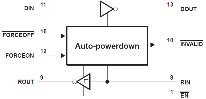
Flexible control options for power management are available when the serial port is inactive. The auto-powerdown feature functions when FORCEON is low and FORCEOFF is high. During this mode of operation, if the devices do not sense a valid RS-232 signal on the receiver input, the driver output is disabled. If FORCEOFF is set low and EN is high, both the driver and receiver are shut off, and the supply current is reduced to 1 μA. Disconnecting the serial port or turning off the peripheral drivers causes the auto-powerdown condition to occur. Auto-powerdown can be disabled when FORCEON and FORCEOFF are high. With auto-powerdown enabled, the device is activated automatically when a valid signal is applied to the receiver input. The INVALID output notifies the user if an RS-232 signal is present at the receiver input. INVALID is high (valid data) if the receiver input voltage is greater than 2.7 V or less than −2.7 V, or has been between −0.3 V and 0.3 V for less than 30 μs. INVALID is low (invalid data) if the receiver input voltage is between −0.3 V and 0.3 V for more than 30 μs. Refer to Figure 7-5 for receiver input levels.
| PART NUMBER | PACKAGE(1) | BODY SIZE (NOM) |
|---|---|---|
| SNx5C3221 | SSOP (DB) 16 | 6.20 mm x 5.30 mm |
| TSSOP (PW) 16 | 10.3 mm x 7.50 mm |
 Logic Diagram (Positive Logic)