SLLSEJ2G July 2015 – March 2020 SN65DP159 , SN75DP159
PRODUCTION DATA.
- 1 Features
- 2 Applications
- 3 Description
- 4 Revision History
- 5 Description (continued)
- 6 Pin Configuration and Functions
-
7 Specifications
- 7.1 Absolute Maximum Ratings
- 7.2 ESD Ratings
- 7.3 Recommended Operating Conditions
- 7.4 Thermal Information
- 7.5 Power Supply Electrical Characteristics
- 7.6 Differential Input Electrical Characteristics
- 7.7 HDMI and DVI TMDS Output Electrical Characteristics
- 7.8 AUX, DDC, and I2C Electrical Characteristics
- 7.9 HPD Electrical Characteristics
- 7.10 HDMI and DVI Main Link Switching Characteristics
- 7.11 AUX Switching Characteristics (Only for RGZ Package)
- 7.12 HPD Switching Characteristics
- 7.13 DDC and I2C Switching Characteristics
- 7.14 Typical Characteristics
- 8 Parameter Measurement Information
-
9 Detailed Description
- 9.1 Overview
- 9.2 Functional Block Diagram
- 9.3
Feature Description
- 9.3.1 Reset Implementation
- 9.3.2 Operation Timing
- 9.3.3 I2C-over-AUX to DDC Bridge (SNx5DP159 48-Pin Package Version Only)
- 9.3.4 Input Lane Swap and Polarity Working
- 9.3.5 Main Link Inputs
- 9.3.6 Main Link Inputs Debug Tools
- 9.3.7 Receiver Equalizer
- 9.3.8 Termination Impedance Control
- 9.3.9 TMDS Outputs
- 9.4 Device Functional Modes
- 9.5 Register Maps
- 10Application and Implementation
- 11Power Supply Recommendations
- 12Layout
- 13Device and Documentation Support
- 14Mechanical, Packaging, and Orderable Information
Package Options
Mechanical Data (Package|Pins)
Thermal pad, mechanical data (Package|Pins)
Orderable Information
9.3.9.1 Pre-Emphasis/De-Emphasis
The SNx5DP159 provides De-emphasis as a way to compensate for the ISI loss between the TMDS outputs and the receiver it is driving. There are two methods to implement this function. When in pin strapping mode the PRE_SEL pin controls this. The PRE_SEL pin provides –2-dB, or 0-dB de-emphasis, which allows output signal pre-conditioning to offset interconnect losses from the SNx5DP159 device outputs to a TMDS receiver. TI recommends setting PRE_SEL at 0 dB while connecting to a receiver through a short PCB route. When pulled to ground with a 65-kΩ resistor –2-dB can be realized, see Figure 9. When using I2C, Reg0Ch[1:0] is used to make these adjustments.
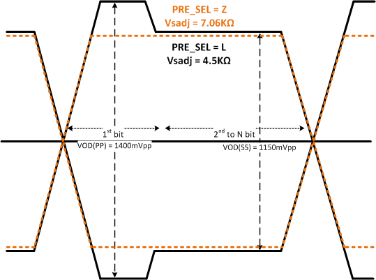
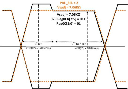
As there are times true pre-emphasis may be the best solution there are two ways to accomplish this. If pin strapping is being use the best method is to reduce the Vsadj resistor value increasing the VOD and then pulling the PRE_SEL pin to ground using the 65-kΩ resistor, see Figure 28. If using I2C this can be accomplished using two methods. First is similar to pin strapping by adjusting the Vsadj resistor value and then implementing –2-dB de-emphasis. Second method is to set Reg0Ch[7:5] = 011 and the set Reg0Ch[1:0] = 01 which accomplishes the same pre-emphasis setting. See Figure 29.
 Figure 28. Pre-Emphasis Using Pin Strapping Method
  Figure 29. Pre-Emphasis Using I2C Method