SLLSEJ2G July 2015 – March 2020 SN65DP159 , SN75DP159
PRODUCTION DATA.
- 1 Features
- 2 Applications
- 3 Description
- 4 Revision History
- 5 Description (continued)
- 6 Pin Configuration and Functions
-
7 Specifications
- 7.1 Absolute Maximum Ratings
- 7.2 ESD Ratings
- 7.3 Recommended Operating Conditions
- 7.4 Thermal Information
- 7.5 Power Supply Electrical Characteristics
- 7.6 Differential Input Electrical Characteristics
- 7.7 HDMI and DVI TMDS Output Electrical Characteristics
- 7.8 AUX, DDC, and I2C Electrical Characteristics
- 7.9 HPD Electrical Characteristics
- 7.10 HDMI and DVI Main Link Switching Characteristics
- 7.11 AUX Switching Characteristics (Only for RGZ Package)
- 7.12 HPD Switching Characteristics
- 7.13 DDC and I2C Switching Characteristics
- 7.14 Typical Characteristics
- 8 Parameter Measurement Information
-
9 Detailed Description
- 9.1 Overview
- 9.2 Functional Block Diagram
- 9.3
Feature Description
- 9.3.1 Reset Implementation
- 9.3.2 Operation Timing
- 9.3.3 I2C-over-AUX to DDC Bridge (SNx5DP159 48-Pin Package Version Only)
- 9.3.4 Input Lane Swap and Polarity Working
- 9.3.5 Main Link Inputs
- 9.3.6 Main Link Inputs Debug Tools
- 9.3.7 Receiver Equalizer
- 9.3.8 Termination Impedance Control
- 9.3.9 TMDS Outputs
- 9.4 Device Functional Modes
- 9.5 Register Maps
- 10Application and Implementation
- 11Power Supply Recommendations
- 12Layout
- 13Device and Documentation Support
- 14Mechanical, Packaging, and Orderable Information
Package Options
Mechanical Data (Package|Pins)
Thermal pad, mechanical data (Package|Pins)
Orderable Information
9.3.9 TMDS Outputs
An 1% precision resistor, 7.06-kΩ, is recommended to be connected from Vsadj pin to ground to allow the differential output swing to comply with TMDS signal levels. The differential output driver provides a typical 10-mA current sink capability when no source term is enabled, which provides a typical 500-mV voltage drop across a 50-Ω termination resistor. As compliance testing is system dependant this resistor value can be adjusted.
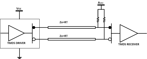
 Figure 27. TMDS Driver and Termination Circuit
 Referring to Figure 27, if both VCC (device supply) and AVCC (sink termination supply) are powered, the TMDS output signals are high impedance when OE = low. The normal operating condition is that both supplies are active. A total of 33-mW of power is consumed by the terminations independent of the OE logical selection. When AVCC is powered on, normal operation (OE controls output impedance) is resumed. When the power source of the device is off and the power source to termination is on, the IO(off) (output leakage current) specification ensures the leakage current is limited 45-μA or less.
The clock and data lanes VOD can be changed through I2C[4] (see VSWING_CLK and VSWING_DATA in Table 8 for details). Figure 3 shows the different output voltage based on different Vsadj resistor values.