SLLSEJ2G July 2015 – March 2020 SN65DP159 , SN75DP159
PRODUCTION DATA.
- 1 Features
- 2 Applications
- 3 Description
- 4 Revision History
- 5 Description (continued)
- 6 Pin Configuration and Functions
-
7 Specifications
- 7.1 Absolute Maximum Ratings
- 7.2 ESD Ratings
- 7.3 Recommended Operating Conditions
- 7.4 Thermal Information
- 7.5 Power Supply Electrical Characteristics
- 7.6 Differential Input Electrical Characteristics
- 7.7 HDMI and DVI TMDS Output Electrical Characteristics
- 7.8 AUX, DDC, and I2C Electrical Characteristics
- 7.9 HPD Electrical Characteristics
- 7.10 HDMI and DVI Main Link Switching Characteristics
- 7.11 AUX Switching Characteristics (Only for RGZ Package)
- 7.12 HPD Switching Characteristics
- 7.13 DDC and I2C Switching Characteristics
- 7.14 Typical Characteristics
- 8 Parameter Measurement Information
-
9 Detailed Description
- 9.1 Overview
- 9.2 Functional Block Diagram
- 9.3
Feature Description
- 9.3.1 Reset Implementation
- 9.3.2 Operation Timing
- 9.3.3 I2C-over-AUX to DDC Bridge (SNx5DP159 48-Pin Package Version Only)
- 9.3.4 Input Lane Swap and Polarity Working
- 9.3.5 Main Link Inputs
- 9.3.6 Main Link Inputs Debug Tools
- 9.3.7 Receiver Equalizer
- 9.3.8 Termination Impedance Control
- 9.3.9 TMDS Outputs
- 9.4 Device Functional Modes
- 9.5 Register Maps
- 10Application and Implementation
- 11Power Supply Recommendations
- 12Layout
- 13Device and Documentation Support
- 14Mechanical, Packaging, and Orderable Information
Package Options
Mechanical Data (Package|Pins)
Thermal pad, mechanical data (Package|Pins)
Orderable Information
9.3.7 Receiver Equalizer
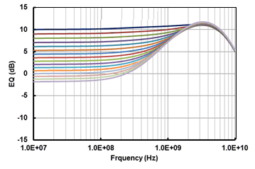
Equalizers are used to clean up inter-symbol interference (ISI) jitter or loss from the bandwidth-limited board traces or cables. The SNx5DP159 device supports both fixed receiver equalizer (redriver and retimer mode) and adaptive receive equalizer (retimer mode) by setting the EQ_SEL/A0 pin or through I2C using reg0Ah[5]. When the EQ_SEL/A0 pin is high, the EQ gain is fixed to 14-dB. The EQ gain will be 7.5-dB if the EQ_SEL/A0 pin is set low. The SNx5DP159 device operates in adaptive equalizer mode when EQ_SEL/A0 left floating. Using adaptive equalization the gain will be automatically adjusted based on the data rate to compensate for variable trace or cable loss. Using the local I2C[4] control, reg0Dh[5:1], the fixed EQ gain can be selected for both data and clock.
 Figure 26. Adaptive EQ Gain Curve