SLLS550E November 2002 – March 2023 SN65HVD08 , SN75HVD08
PRODUCTION DATA
- 1 Features
- 2 Applications
- 3 Description
- 4 Revision History
- 5 Pin Configuration and Functions
- 6 Specifications
- 7 Parameter Measurement Information
- 8 Detailed Description
- 9 Application and Implementation
- 10Device and Documentation Support
- 11Mechanical, Packaging, and Orderable Information
Package Options
Mechanical Data (Package|Pins)
- P|8
Thermal pad, mechanical data (Package|Pins)
Orderable Information
3 Description
The SN65HVD08 combines a 3-state differential line driver and differential line receiver designed for balanced data transmission and interoperation with ANSI TIA/EIA-485-A and ISO-8482E standard-compliant devices.
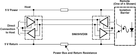
The wide supply voltage range and low quiescent current requirements allow the SN65HVD08s to operate from a 5-V power bus in the cable with as much as a 2-V line voltage drop. Busing power in the cable can alleviate the need for isolated power to be generated at each connection of a ground-isolated bus.
The driver differential outputs and receiver differential inputs connect internally to form a differential input/output (I/O) bus port that is designed to offer minimum loading to the bus whenever the driver is disabled or not powered. The drivers and receivers have active-high and active-low enables respectively, which can be externally connected together to function as a direction control.
| PART NUMBER | PACKAGE(1) | BODY SIZE (NOM) |
|---|---|---|
| SN75HVD08, SN65HVD08 | SOIC (8) | 4.90 mm × 3.91 mm |
| PDIP (8) | 9.81 mm × 6.35 mm |
 Typical Application Schematic