SLLS550E November 2002 – March 2023 SN65HVD08 , SN75HVD08
PRODUCTION DATA
- 1 Features
- 2 Applications
- 3 Description
- 4 Revision History
- 5 Pin Configuration and Functions
- 6 Specifications
- 7 Parameter Measurement Information
- 8 Detailed Description
- 9 Application and Implementation
- 10Device and Documentation Support
- 11Mechanical, Packaging, and Orderable Information
Package Options
Mechanical Data (Package|Pins)
- P|8
Thermal pad, mechanical data (Package|Pins)
Orderable Information
5 Pin Configuration and Functions
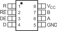
 Figure 5-1 D or P Package, 8-Pin SOIC or
PDIP
Figure 5-1 D or P Package, 8-Pin SOIC or
PDIP(Top View)
Table 5-1 Pin Functions
| PIN | TYPE | DESCRIPTION | |
|---|---|---|---|
| NAME | NO. | ||
| A | 6 | Bus input / output | Driver output and receiver input (complementary to B) |
| B | 7 | Bus input / output | Driver output and receiver input (complementary to A) |
| D | 4 | Digital input | Driver data input |
| DE | 3 | Digital input | Driver enable high |
| GND | 5 | Reference potential | Local device ground |
| R | 1 | Digital output | Receive data output |
| RE | 2 | Digital input | Receiver enable low |
| VCC | 8 | Supply | 3-V to 5.5-V supply |