SLLS550E November 2002 – March 2023 SN65HVD08 , SN75HVD08
PRODUCTION DATA
- 1 Features
- 2 Applications
- 3 Description
- 4 Revision History
- 5 Pin Configuration and Functions
- 6 Specifications
- 7 Parameter Measurement Information
- 8 Detailed Description
- 9 Application and Implementation
- 10Device and Documentation Support
- 11Mechanical, Packaging, and Orderable Information
Package Options
Mechanical Data (Package|Pins)
- P|8
Thermal pad, mechanical data (Package|Pins)
Orderable Information
6.7 Receiver Switching Characteristics
over recommended operating conditions unless otherwise noted
| PARAMETER | TEST CONDITIONS | MIN | TYP | MAX | UNIT | |
|---|---|---|---|---|---|---|
| tPHL | Receiver high-to-low propagation delay time | CL = 15 pF, See Figure 7-6 | 70 | ns | ||
| tPLH | Receiver low-to-high propagation delay time | 70 | ||||
| tr | Receiver 10%-to-90% differential output rise time | 5 | ||||
| tf | Receiver 90%-to-10% differential output fall time | 5 | ||||
| tSK(P) | Receiver differential output pulse skew, |tPHL - tPLH| | 4.5 | ||||
| ten | Receiver enable time | Driver enabled, See Figure 7-7 | 15 | ns | ||
| Driver disabled, See Figure 7-8 | 6 | µs | ||||
| tdis | Receiver disable time | Driver enabled, See Figure 7-7 | 20 | ns | ||
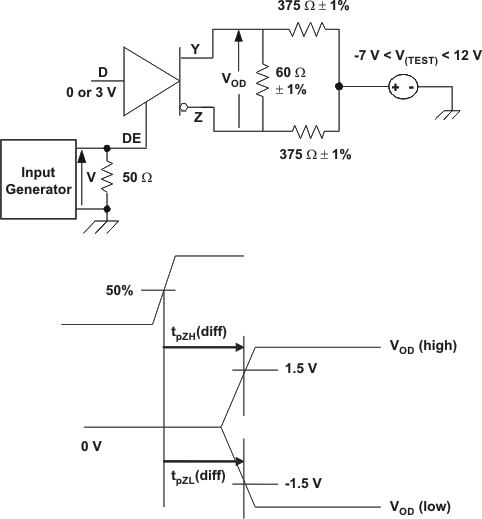
 Figure 6-1 Driver Enable Time From DE to VOD
The time tpZL(x) is the measure from DE to VOD(x). VOD is valid when it is greater than 1.5 V.