SLLS376G May 2000 – February 2023 SN65LBC176A , SN75LBC176A
PRODUCTION DATA
- 1Features
- 2Description
- 3Revision History
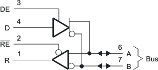
- 4Pin Configuration and Functions
- 5Specifications
- 6Detailed Description
- 7Device and Documentation Support
- 8Mechanical, Packaging, and Orderable Information
Package Options
Mechanical Data (Package|Pins)
- P|8
Thermal pad, mechanical data (Package|Pins)
Orderable Information
2 Description
The SN65LBC176A, SN65LBC176AQ, and SN75LBC176A differential bus transceivers are monolithic, integrated circuits designed for bidirectional data communication on multipoint bus-transmission lines. They are designed for balanced transmission lines and are compatible with ANSI standard TIA/EIA-485-A and ISO 8482. The A version offers improved switching performance over its predecessors without sacrificing significantly more power.
The SN65LBC176A, SN65LBC176AQ, and SN75LBC176A combine a 3-state, differential line driver and a differential input line receiver, both of which operate from a single 5-V power supply. The driver and receiver have active-high and active-low enables, respectively, which can externally connect together to function as a direction control. The driver differential outputs and the receiver differential inputs connect internally to form a differential input /output (I/O) bus port that is designed to offer minimum loading to the bus whenever the driver is disabled or VCC = 0. This port features wide positive and negative common-mode voltage ranges, making the device suitable for party-line applications. Very low device supply current can be achieved by disabling the driver and the receiver.
| PART NUMBER | PACKAGE(1) | BODY SIZE (NOM) |
|---|---|---|
| SN65LBC176A SN75LBC176A |
D (SOIC) | 4.9 mm x 3.91 mm |
| P (PDIP) | 9.81 mm x 6.35 mm |