SLLS846C May 2009 – August 2014 SN75LVDS83B
PRODUCTION DATA.
- 1 Features
- 2 Applications
- 3 Description
- 4 Revision History
- 5 Description (Continued)
- 6 Pin Configuration and Functions
- 7 Specifications
- 8 Parameter Measurement Information
- 9 Detailed Description
- 10Application and Implementation
- 11Power Supply Recommendations
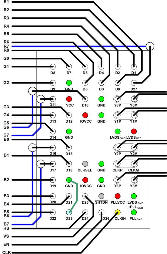
- 12Layout
- 13Device and Documentation Support
- 14Mechanical, Packaging, and Orderable Information
Package Options
Mechanical Data (Package|Pins)
- DGG|56
Thermal pad, mechanical data (Package|Pins)
Orderable Information
10 Application and Implementation
10.1 Application Information
This section describes the power up sequence, provides information on device connectivity to various GPU and LCD display panels, and offers a PCB routing example.
10.2 Typical Application
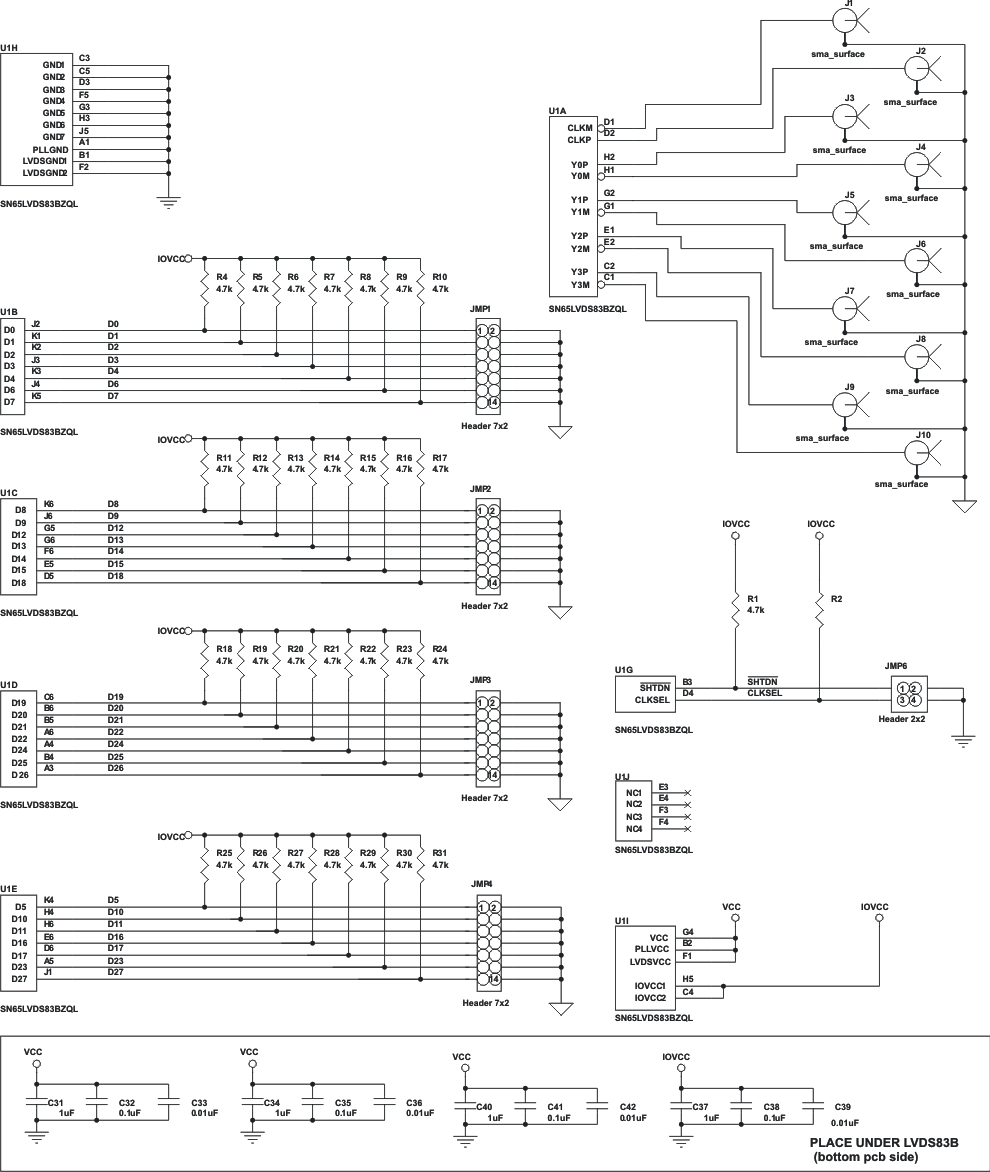 Figure 14. Schematic Example (SN75LVDS83B Evaluation Board)
10.2.1 Design Requirements
| DESIGN PARAMETER | EXAMPLE VALUE |
|---|---|
| VCC | 3.3 V |
| VCCIO | 1.8 V |
| CLKIN | Falling edge |
| SHTDN# | High |
| Format | 18-bit GPU to 24-bit LCD |
10.2.2 Detailed Design Procedure
10.2.2.1 Power Up Sequence
The SN75LVDS83B does not require a specific power up sequence.
It is permitted to power up IOVCC while VCC, VCCPLL, and VCCLVDS remain powered down and connected to GND. The input level of the SHTDN during this time does not matter as only the input stage is powered up while all other device blocks are still powered down.
It is also permitted to power up all 3.3V power domains while IOVCC is still powered down to GND. The device will not suffer damage. However, in this case, all the I/Os are detected as logic HIGH, regardless of their true input voltage level. Hence, connecting SHTDN to GND will still be interpreted as a logic HIGH; the LVDS output stage will turn on. The power consumption in this condition is significantly higher than standby mode, but still lower than normal mode.
The user experience can be impacted by the way a system powers up and powers down an LCD screen. The following sequence is recommended:
Power up sequence (SN75LVDS83B SHTDN input initially low):
- Ramp up LCD power (maybe 0.5ms to 10ms) but keep backlight turned off.
- Wait for additional 0-200ms to ensure display noise won’t occur.
- Enable video source output; start sending black video data.
- Toggle LVDS83B shutdown to SHTDN = VIH.
- Send >1ms of black video data; this allows the LVDS83B to be phase locked, and the display to show black data first.
- Start sending true image data.
- Enable backlight.
Power Down sequence (SN75LVDS83B SHTDN input initially high):
- Disable LCD backlight; wait for the minimum time specified in the LCD data sheet for the backlight to go low.
- Video source output data switch from active video data to black image data (all visible pixel turn black); drive this for >2 frame times.
- Set SN75LVDS83B input SHTDN = GND; wait for 250ns.
- Disable the video output of the video source.
- Remove power from the LCD panel for lowest system power.
10.2.2.2 Signal Connectivity
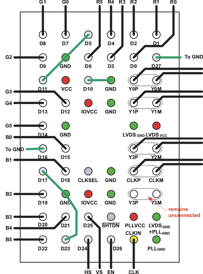
While there is no formal industry standardized specification for the input interface of LVDS LCD panels, the industry has aligned over the years on a certain data format (bit order). Figure 15 through Figure 18 show how each signal should be connected from the graphic source through the SN75LVDS83B input, output and LVDS LCD panel input. Detailed notes are provided with each figure.
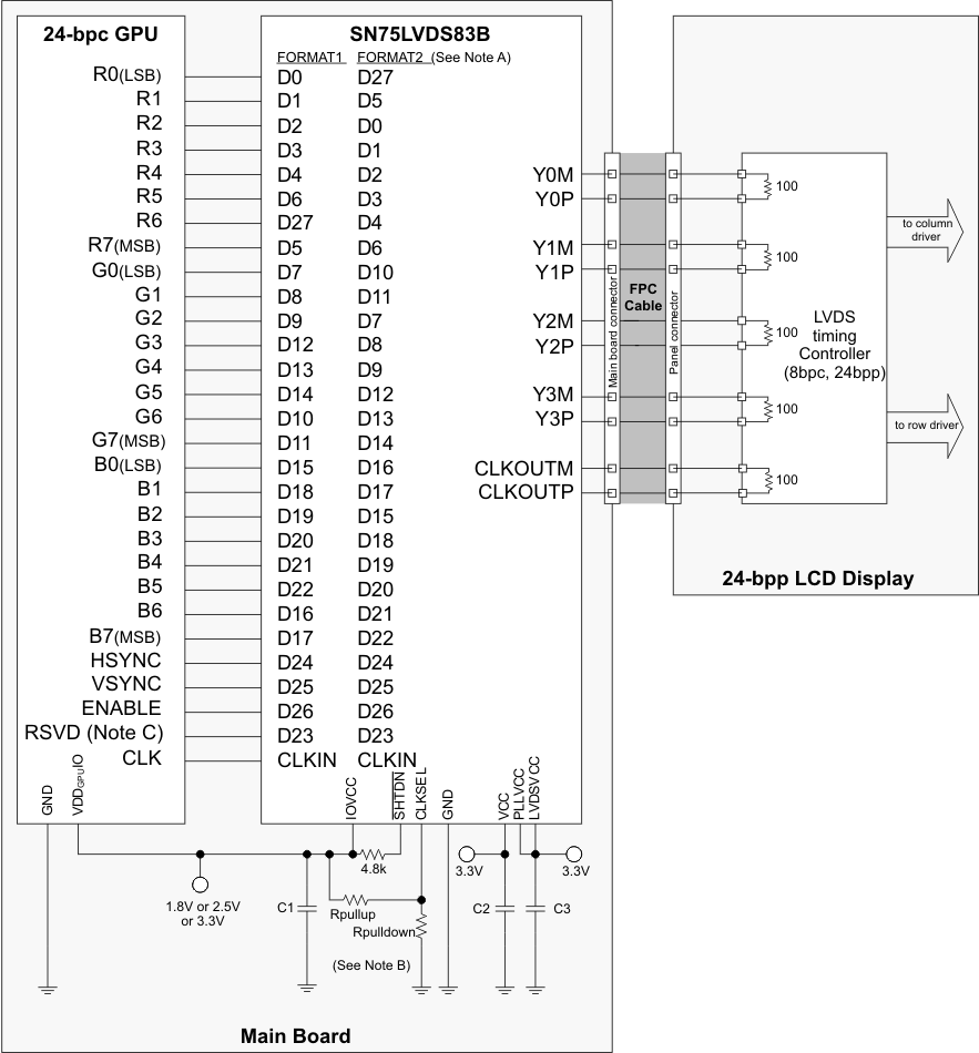
- Format 1: use with displays expecting the 2 MSB to be transmitted over the 4th data channel Y3. This is the dominate data format for LCD panels.
- Format 2: use with displays expecting the 2 LSB to be transmitted over the 4th data channel.
Rpulldown: install only to use falling edge triggered clocking.
- C1: decoupling cap for the VDDIO supply; install at least 1x0.01µF.
- C2: decoupling cap for the VDD supply; install at least 1x0.1µF and 1x0.01µF.
- C3: decoupling cap for the VDDPLL and VDDLVDS supply; install at least 1x0.1µF and 1x0.01µF.
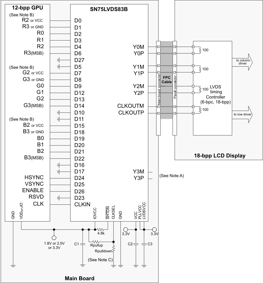
R2, G2, B2: these outputs also connects to the LSB of each color for increased, dynamic range of the entire color space at the expense of none-linear step sizes between each step. For linear steps with less dynamic range, connect D0, D7, and D15 to VCC.
Rpulldown: install only to use falling edge triggered clocking.
- C1: decoupling cap for the VDDIO supply; install at least 1x0.01µF.
- C2: decoupling cap for the VDD supply; install at least 1x0.1µF and 1x0.01µF.
- C3: decoupling cap for the VDDPLL and VDDLVDS supply; install at least 1x0.1µF and 1x0.01µF.
10.2.3 Application Curve
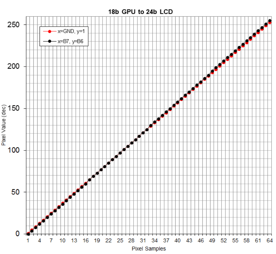 Figure 21. 18b GPU to 24b LCD