SLLS846C May 2009 – August 2014 SN75LVDS83B
PRODUCTION DATA.
- 1 Features
- 2 Applications
- 3 Description
- 4 Revision History
- 5 Description (Continued)
- 6 Pin Configuration and Functions
- 7 Specifications
- 8 Parameter Measurement Information
- 9 Detailed Description
- 10Application and Implementation
- 11Power Supply Recommendations
- 12Layout
- 13Device and Documentation Support
- 14Mechanical, Packaging, and Orderable Information
Package Options
Mechanical Data (Package|Pins)
- DGG|56
Thermal pad, mechanical data (Package|Pins)
Orderable Information
12 Layout
12.1 Layout Guidelines
12.1.1 Board Stackup
There is no fundamental information about how many layers should be used and how the board stackup should look. Again, the easiest way the get good results is to use the design from the EVMs of Texas Instruments. The magazine Elektronik Praxis has published an article with an analysis of different board stackups. These are listed in Table 3. Generally, the use of microstrip traces needs at least two layers, whereas one of them must be a GND plane. Better is the use of a four-layer PCB, with a GND and a VCC plane and two signal layers. If the circuit is complex and signals must be routed as stripline, because of propagation delay and/or characteristic impedance, a six-layer stackup should be used.
Table 3. Possible Board Stackup on a Four-Layer PCB
| MODEL 1 | MODEL 2 | MODEL 3 | MODEL 4 | |
|---|---|---|---|---|
| Layer 1 | SIG | SIG | SIG | GND |
| Layer 2 | SIG | GND | GND | SIG |
| Layer 3 | VCC | VCC | SIG | VCC |
| Layer 4 | GND | SIG | VCC | SIG |
| Decoupling | Good | Good | Bad | Bad |
| EMC | Bad | Bad | Bad | Bad |
| Signal Integrity | Bad | Bad | Good | Bad |
| Self Disturbance | Satisfaction | Satisfaction | Satisfaction | High |
12.1.2 Power and Ground Planes
A complete ground plane in high-speed design is essential. Additionally, a complete power plane is recommended as well. In a complex system, several regulated voltages can be present. The best solution is for every voltage to have its own layer and its own ground plane. But this would result in a huge number of layers just for ground and supply voltages. What are the alternatives? Split the ground planes and the power planes? In a mixed-signal design, e.g., using data converters, the manufacturer often recommends splitting the analog ground and the digital ground to avoid noise coupling between the digital part and the sensitive analog part. Take care when using split ground planes because:
- Split ground planes act as slot antennas and radiate.
- A routed trace over a gap creates large loop areas, because the return current cannot flow beside the signal, and the signal can induce noise into the nonrelated reference plane (Figure 22).
- With a proper signal routing, crosstalk also can arise in the return current path due to discontinuities in the ground plane. Always take care of the return current (Figure 23).
For Figure 23, do not route a signal referenced to digital ground over analog ground and vice versa. The return current cannot take the direct way along the signal trace and so a loop area occurs. Furthermore, the signal induces noise, due to crosstalk (dotted red line) into the analog ground plane.
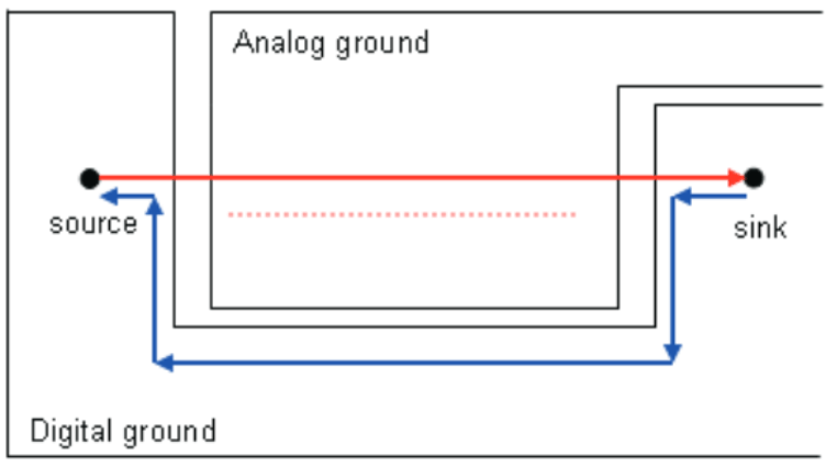 Figure 22. Loop Area and Crosstalk Due to Poor Signal Routing and Ground Splitting
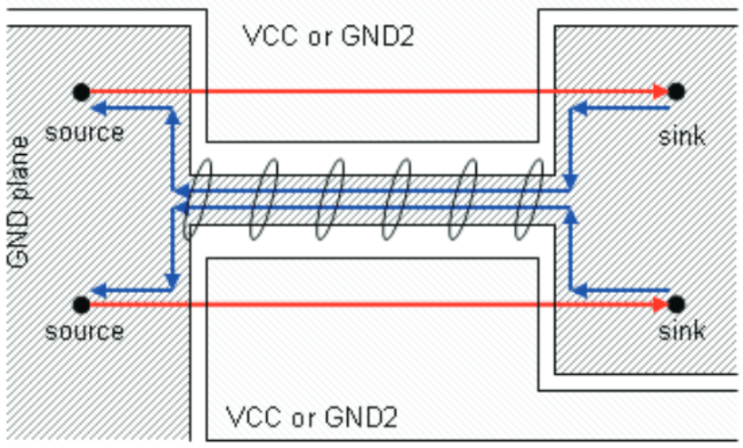 Figure 23. Crosstalk Induced by the Return Current Path
12.1.3 Traces, Vias, and Other PCB Components
A right angle in a trace can cause more radiation. The capacitance increases in the region of the corner, and the characteristic impedance changes. This impedance change causes reflections.
- Avoid right-angle bends in a trace and try to route them at least with two 45° corners. To minimize any impedance change, the best routing would be a round bend (see Figure 24).
- Separate high-speed signals (e.g., clock signals) from low-speed signals and digital from analog signals; again, placement is important.
- To minimize crosstalk not only between two signals on one layer but also between adjacent layers, route them with 90° to each other.
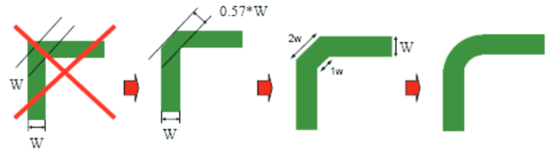 Figure 24. Poor and Good Right Angle Bends
12.2 Layout Example
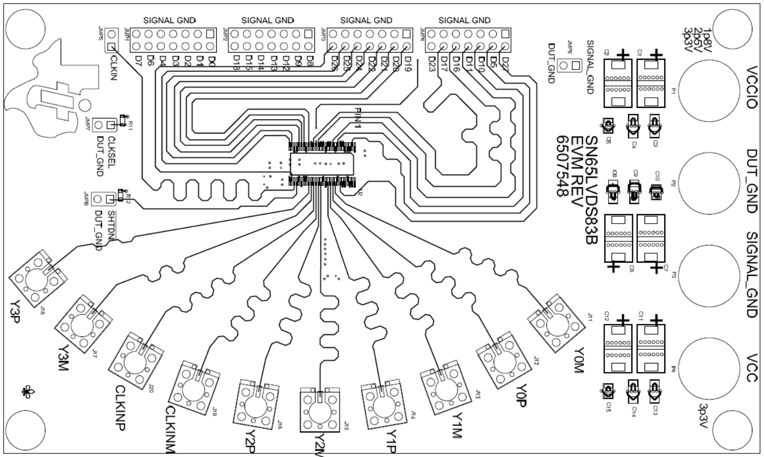 Figure 25. SN75LVDS83B EVM Top Layer – TSSOP Package
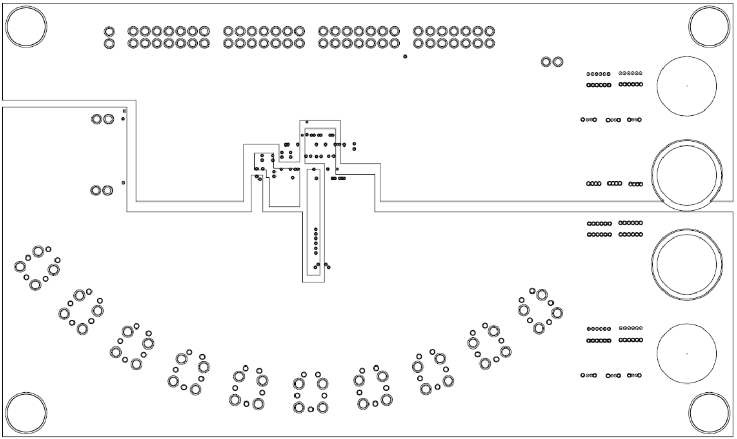 Figure 26. SN75LVDS83B EVM VCC Layer – TSSOP Package