SLLS846C May 2009 – August 2014 SN75LVDS83B
PRODUCTION DATA.
- 1 Features
- 2 Applications
- 3 Description
- 4 Revision History
- 5 Description (Continued)
- 6 Pin Configuration and Functions
- 7 Specifications
- 8 Parameter Measurement Information
- 9 Detailed Description
- 10Application and Implementation
- 11Power Supply Recommendations
- 12Layout
- 13Device and Documentation Support
- 14Mechanical, Packaging, and Orderable Information
Package Options
Mechanical Data (Package|Pins)
- DGG|56
Thermal pad, mechanical data (Package|Pins)
Orderable Information
7 Specifications
7.1 Absolute Maximum Ratings(1)
| MIN | MAX | UNIT | ||
|---|---|---|---|---|
| Supply voltage range, VCC, IOVCC, LVDSVCC, PLLVCC(2) | –0.5 | 4 | V | |
| Voltage range at any output terminal | –0.5 | VCC + 0.5 | V | |
| Voltage range at any input terminal | –0.5 | IOVCC + 0.5 | V | |
| Continuous power dissipation | See Dissipation Ratings | |||
(1) Stresses above these ratings may cause permanent damage. Exposure to absolute maximum conditions for extended periods may degrade device reliability. These are stress ratings only, and functional operation of the device at these or any other conditions beyond those specified is not implied.
(2) All voltages are with respect to the GND terminals.
7.2 Handling Ratings
| MIN | MAX | UNIT | |||
|---|---|---|---|---|---|
| Tstg | Storage temperature range | –65 | 150 | °C | |
| V(ESD) | Electrostatic discharge | Human Body Model (HBM)(1) all pins | 5 | kV | |
| Charged Device Model (CDM)(2) all pins | 500 | V | |||
| Machine Model (MM)(3) all pins | 150 | ||||
(1) In accordance with JEDEC Standard 22, Test Method A114-A.
(2) In accordance with JEDEC Standard 22, Test Method C101.
(3) In accordance with JEDEC Standard 22, Test Method A115-A.
7.3 Recommended Operating Conditions
over operating free-air temperature range (unless otherwise noted)| PARAMETER | MIN | NOM | MAX | UNIT | |
|---|---|---|---|---|---|
| Supply voltage, VCC | 3 | 3.3 | 3.6 | V | |
| LVDS output Supply voltage, LVDSVCC | 3 | 3.3 | 3.6 | ||
| PLL analog supply voltage, PLLVCC | 3 | 3.3 | 3.6 | ||
| IO input reference supply voltage, IOVCC | 1.62 | 1.8 / 2.5 / 3.3 | 3.6 | ||
| Power supply noise on any VCC terminal | 0.1 | ||||
| High-level input voltage, VIH | IOVCC = 1.8 V | IOVCC/2 + 0.3 V | V | ||
| IOVCC = 2.5 V | IOVCC/2 + 0.4 V | ||||
| IOVCC = 3.3 V | IOVCC/2 + 0.5 V | ||||
| Low-level input voltage, VIL | IOVCC = 1.8 V | IOVCC/2 - 0.3 V | V | ||
| IOVCC = 2.5 V | IOVCC/2 - 0.4 V | ||||
| IOVCC = 3.3 V | IOVCC/2 - 0.5 V | ||||
| Differential load impedance, ZL | 90 | 132 | Ω | ||
| Operating free-air temperature, TA | –10 | 70 | C | ||
7.4 Thermal Information
over operating free-air temperature range (unless otherwise noted)| PARAMETER | TEST CONDITIONS | ZQL | DGG | UNIT | |||||
|---|---|---|---|---|---|---|---|---|---|
| MIN | TYP | MAX | MIN | TYP | MAX | ||||
| θJA | Junction-to-free-air thermal resistance | Low-K JEDEC test board, 1s (single signal layer), no air flow | 85 | °C/W | |||||
| High-K JEDEC test board, 2s2p (double signal layer, double buried power plane), no air flow | 67.1 | 63.4 | |||||||
| θJC | Junction-to-case thermal resistance | Cu cold plate measurement process | 25.2 | 15.9 | °C/W | ||||
| θJB | Junction-to-board thermal resistance | EIA/JESD 51-8 | 31.0 | 32.5 | °C/W | ||||
| ψJT | Junction-to-top of package | EIA/JESD 51-2 | 0.8 | 0.4 | °C/W | ||||
| ψJB | Junction-to-board | EIA/JESD 51-6 | 30.3 | 32.2 | °C/W | ||||
| TA | Operating ambient temperature range | –10 | 70 | –10 | 70 | °C | |||
| TJ | Virtual junction temperature | 0 | 105 | 0 | 105 | °C | |||
7.5 Dissipation Ratings
| PACKAGE | CIRCUIT BOARD MODEL(1) | TJA ≤ 25°C | DERATING FACTOR(2)
ABOVE TJA = 25°C |
TJA = 70°C POWER RATING |
|---|---|---|---|---|
| DGG | Low-K | 1111 mW | 12.3 mW/°C | 555 mW |
| ZQL | 1034 mW | 11.5 mW/°C | 517 mW | |
| DGG(3) | High-K | 1730 mW | 19 mW/°C | 865 mW |
| ZQL | 2000 mW | 22 mW/°C | 1000 mW |
(1) In accordance with the High-K and Low-K thermal metric definitions of EIA/JESD51-2.
(2) This is the inverse of the junction-to-ambient thermal resistance when board-mounted and with no air flow.
7.6 Electrical Characteristics
over operating free-air temperature range (unless otherwise noted)| PARAMETER | TEST CONDITIONS | MIN | TYP(1) | MAX | UNIT | |
|---|---|---|---|---|---|---|
| VT | Input voltage threshold | RL = 100Ω, See Figure 7 | IOVCC/2 | V | ||
| |VOD| | Differential steady-state output voltage magnitude | 250 | 450 | mV | ||
| Δ|VOD| | Change in the steady-state differential output voltage magnitude between opposite binary states | 1 | 35 | mV | ||
| VOC(SS) | Steady-state common-mode output voltage | See Figure 7
tR/F (Dx, CLKin) = 1ns |
1.125 | 1.375 | V | |
| VOC(PP) | Peak-to-peak common-mode output voltage | 35 | mV | |||
| IIH | High-level input current | VIH = IOVCC | 25 | μA | ||
| IIL | Low-level input current | VIL = 0 V | ±10 | μA | ||
| IOS | Short-circuit output current | VOY = 0 V | ±24 | mA | ||
| VOD = 0 V | ±12 | mA | ||||
| IOZ | High-impedance state output current | VO = 0 V to VCC | ±20 | μA | ||
| Rpdn | Input pull-down integrated resistor on all inputs (Dx, CLKSEL, SHTDN, CLKIN) | IOVCC = 1.8 V | 200 | kΩ | ||
| IOVCC = 3.3 V | 100 | |||||
| IQ | Quiescent current (average) | disabled, all inputs at GND; SHTDN = VIL |
2 | 100 | μA | |
| ICC | Supply current (average) | SHTDN = VIH, RL = 100Ω (5 places), grayscale pattern (Figure 8) VCC = 3.3 V, fCLK = 75 MHz |
||||
| I(VCC) + I(PLLVCC) + I(LVDSVCC) | 51.9 | mA | ||||
| I(IOVCC) with IOVCC = 3.3 V | 0.4 | |||||
| I(IOVCC) with IOVCC = 1.8 V | 0.1 | |||||
| SHTDN = VIH, RL = 100Ω (5 places), 50% transition density pattern (Figure 8), VCC = 3.3 V, fCLK = 75 MHz |
||||||
| I(VCC) + I(PLLVCC) + I(LVDSVCC) | 53.3 | mA | ||||
| I(IOVCC) with IOVCC = 3.3 V | 0.6 | |||||
| I(IOVCC) with IOVCC = 1.8 V | 0.2 | |||||
| SHTDN = VIH, RL = 100Ω (5 places), worst-case pattern (Figure 9), VCC = 3.6 V, fCLK = 75 MHz |
||||||
| I(VCC) + I(PLLVCC) + I(LVDSVCC) | 63.7 | mA | ||||
| I(IOVCC) with IOVCC = 3.3 V | 1.3 | |||||
| I(IOVCC) with IOVCC = 1.8 V | 0.5 | |||||
| SHTDN = VIH, RL = 100Ω (5 places), worst-case pattern (Figure 9), fCLK = 100 MHz |
||||||
| I(VCC) + I(PLLVCC) + I(LVDSVCC) | 81.6 | mA | ||||
| I(IOVCC) with IOVCC = 3.6 V | 1.6 | |||||
| I(IOVCC) with IOVCC = 1.8 V | 0.6 | |||||
| SHTDN = VIH, RL = 100Ω (5 places), worst-case pattern (Figure 9), fCLK = 135 MHz |
||||||
| I(VCC) + I(PLLVCC) + I(LVDSVCC) | 102.2 | mA | ||||
| I(IOVCC) with IOVCC = 3.6 V | 2.1 | |||||
| I(IOVCC) with IOVCC = 1.8 V | 0.8 | |||||
| CI | Input capacitance | 2 | pF | |||
(1) All typical values are at VCC = 3.3 V, TA = 25°C.
7.7 Timing Requirements
| PARAMETER | MIN | MAX | UNIT | |
|---|---|---|---|---|
| Input clock period, tc | 7.4 | 100 | ns | |
| Input clock modulation | with modulation frequency 30 kHz | 8% | ||
| with modulation frequency 50 kHz | 6% | |||
| High-level input clock pulse width duration, tw | 0.4 tc | 0.6 tc | ns | |
| Input signal transition time, tt | 3 | ns | ||
| Data set up time, D0 through D27 before CLKIN (See Figure 6) | 2 | ns | ||
| Data hold time, D0 through D27 after CLKIN | 0.8 | ns | ||
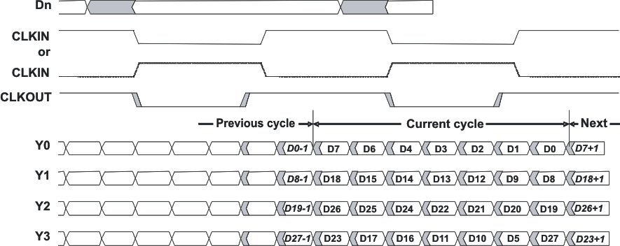 Figure 1. Typical SN75LVDS83B Load and Shift Sequences
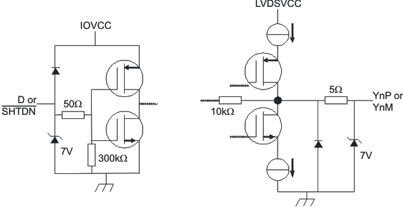 Figure 2. Equivalent Input and Output Schematic Diagrams
7.8 Switching Characteristics
over operating free-air temperature range (unless otherwise noted)| PARAMETER | TEST CONDITIONS | MIN | TYP(1) | MAX | UNIT | |
|---|---|---|---|---|---|---|
| t0 | Delay time, CLKOUT↑ after Yn valid (serial bit position 0, equal D1, D9, D20, D5) | See Figure 10, tC = 10ns, |Input clock jitter| < 25ps (2) |
-0.1 | 0 | 0.1 | ns |
| t1 | Delay time, CLKOUT↑ after Yn valid (serial bit position 1, equal D0, D8, D19, D27) | 1/7 tc - 0.1 | 1/7 tc + 0.1 | ns | ||
| t2 | Delay time, CLKOUT↑ after Yn valid (serial bit position 2, equal D7, D18, D26. D23) | 2/7 tc - 0.1 | 2/7 tc + 0.1 | ns | ||
| t3 | Delay time, CLKOUT↑ after Yn valid (serial bit position 3; equal D6, D15, D25, D17) | 3/7 tc - 0.1 | 3/7 tc + 0.1 | ns | ||
| t4 | Delay time, CLKOUT↑ after Yn valid (serial bit position 4, equal D4, D14, D24, D16) | 4/7 tc - 0.1 | 4/7 tc + 0.1 | ns | ||
| t5 | Delay time, CLKOUT↑ after Yn valid (serial bit position 5, equal D3, D13, D22, D11) | 5/7 tc - 0.1 | 5/7 tc + 0.1 | ns | ||
| t6 | Delay time, CLKOUT↑ after Yn valid (serial bit position 6, equal D2, D12, D21, D10) | 6/7 tc - 0.1 | 6/7 tc + 0.1 | ns | ||
| tc(o) | Output clock period | tc | ns | |||
| Δtc(o) | Output clock cycle-to-cycle jitter (3) | tC = 10ns; clean reference clock, see Figure 11 | ±26 | ps | ||
| tC = 10ns with 0.05UI added noise modulated at 3MHz, see Figure 11 | ±44 | |||||
| tC = 7.4ns; clean reference clock, see Figure 11 | ±35 | |||||
| tC = 7.4ns with 0.05UI added noise modulated at 3MHz, see Figure 11 | ±42 | |||||
| tw | High-level output clock pulse duration | 4/7 tc | ns | |||
| tr/f | Differential output voltage transition time (tr or tf) | See Figure 7 | 225 | 500 | ps | |
| ten | Enable time, SHTDN↑ to phase lock (Yn valid) | f(clk) = 135 MHz, See Figure 12 | 6 | µs | ||
| tdis | Disable time, SHTDN↓ to off-state (CLKOUT high-impedance) | f(clk) = 135 MHz, See Figure 13 | 7 | ns | ||
(1) All typical values are at VCC = 3.3 V, TA = 25°C.
(2) |Input clock jitter| is the magnitude of the change in the input clock period.
7.9 Typical Characteristics
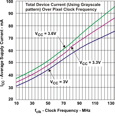 Figure 3. Average Grayscale ICC vs Clock Frequency
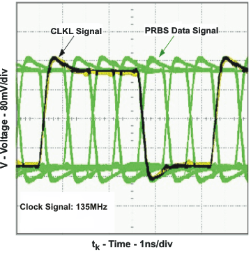 Figure 5. Typical PRBS Output Signal Over One Clock Period
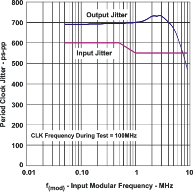 Figure 4. Output Clock Jitter vs Input Clock Jitter