SLASF30 January 2022 TAA5212
ADVANCE INFORMATION
- 1
- 1 Features
- 2 Applications
- 3 Description
- 4 Revision History
- 5 Pin Configuration and Functions
-
6 Specifications
- 6.1 Absolute Maximum Ratings
- 6.2 ESD Ratings
- 6.3 Recommended Operating Conditions
- 6.4 Thermal Information
- 6.5 Electrical Characteristics
- 6.6 Timing Requirements: I2C Interface
- 6.7 Switching Characteristics: I2C Interface
- 6.8 Timing Requirements: SPI Interface
- 6.9 Switching Characteristics: SPI Interface
- 6.10 Timing Requirements: TDM, I2S or LJ Interface
- 6.11 Switching Characteristics: TDM, I2S or LJ Interface
- 6.12 Timing Requirements: PDM Digital Microphone Interface
- 6.13 Switching Characteristics: PDM Digial Microphone Interface
- 7 Parameter Measurement Information
-
8 Detailed Description
- 8.1 Overview
- 8.2 Functional Block Diagram
- 8.3
Feature Description
- 8.3.1 Hardware Control
- 8.3.2 Serial Interfaces
- 8.3.3 Phase-Locked Loop (PLL) and Clock Generation
- 8.3.4 Input Channel Configurations
- 8.3.5 Reference Voltage
- 8.3.6 Programmable Microphone Bias
- 8.3.7
Signal-Chain Processing
- 8.3.7.1
ADC Signal-Chain
- 8.3.7.1.1 Programmable Channel Gain and Digital Volume Control
- 8.3.7.1.2 Programmable Channel Gain Calibration
- 8.3.7.1.3 Programmable Channel Phase Calibration
- 8.3.7.1.4 Programmable Digital High-Pass Filter
- 8.3.7.1.5 Programmable Digital Biquad Filters
- 8.3.7.1.6 Programmable Channel Summer and Digital Mixer
- 8.3.7.1.7 Configurable Digital Decimation Filters
- 8.3.7.1
ADC Signal-Chain
- 8.3.8 Interrupts, Status, and Digital I/O Pin Multiplexing
- 8.3.9 Programmable Channel Phase Calibration
- 8.4 Device Functional Modes
- 8.5 Register Maps
- 8.6 Feature Description
- 8.7 Device Functional Modes
- 9 Application and Implementation
- 10Power Supply Recommendations
- 11Layout
- 12Device and Documentation Support
- 13Mechanical, Packaging, and Orderable Information
Package Options
Mechanical Data (Package|Pins)
- RGE|24
Thermal pad, mechanical data (Package|Pins)
Orderable Information
8.3.7.1.4 Programmable Digital High-Pass Filter
To remove the DC offset component and attenuate the undesired low-frequency noise content in the record data, the device supports a programmable high-pass filter (HPF). The HPF is not a channel-independent filter setting but is globally applicable for all ADC channels. This HPF is constructed using the first-order infinite impulse response (IIR) filter, and is efficient enough to filter out possible DC components of the signal. Table 8-15 shows the predefined –3-dB cutoff frequencies available that can be set by using the ADC_DSP_HPF_SEL[1:0] register bits of P0_R114. Additionally, to achieve a custom –3-dB cutoff frequency for a specific application, the device also allows the first-order IIR filter coefficients to be programmed when the HPF_SEL[1:0] register bits are set to 2'b00. Figure 8-18 illustrates a frequency response plot for the HPF filter.
| P0_R107_D[1:0] : HPF_SEL[1:0] | -3-dB CUTOFF FREQUENCY SETTING | -3-dB CUTOFF FREQUENCY AT 16-kHz SAMPLE RATE | -3-dB
CUTOFF FREQUENCY AT 48-kHz SAMPLE RATE |
|---|---|---|---|
| 00 | Programmable 1st-order IIR filter | Programmable 1st-order IIR filter | Programmable 1st-order IIR filter |
| 01 (default) | 0.00002 × fS | 0.25 Hz | 1 Hz |
| 10 | 0.00025 × fS | 4 Hz | 12 Hz |
| 11 | 0.002 × fS | 32 Hz | 96 Hz |
 Figure 8-18 HPF
Filter Frequency Response Plot
Figure 8-18 HPF
Filter Frequency Response PlotEquation 1 gives the transfer function for the first-order programable IIR filter:
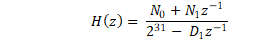
The frequency response for this first-order programmable IIR filter with default coefficients is flat at a gain of 0 dB (all-pass filter). The host device can override the frequency response by programming the IIR coefficients in Table 8-16 to achieve the desired frequency response for high-pass filtering or any other desired filtering. If HPF_SEL[1:0] are set to 2'b00, the host device must write these coefficients values for the desired frequency response before powering-up any ADC channel for recording. Table 8-16 shows the filter coefficients for the first-order IIR filter.
| FILTER | FILTER COEFFICIENT | DEFAULT COEFFICIENT VALUE | COEFFICIENT REGISTER MAPPING |
|---|---|---|---|
| Programmable 1st-order IIR filter (can be allocated to HPF or any other desired filter) | N0 | 0x7FFFFFFF | P4_R72-R75 |
| N1 | 0x00000000 | P4_R76-R79 | |
| D1 | 0x00000000 | P4_R80-R83 |