SLAS978B September 2013 – February 2014 TAS2553
PRODUCTION DATA.
- 1 Features
- 2 Applications
- 3 Description
- 4 Revision History
- 5 Terminal Configuration and Functions
- 6 Specifications
-
7 Detailed Description
- 7.1 Overview
- 7.2 Functional Block Diagram
- 7.3 Feature Description
- 7.4 Device Functional Modes
- 7.5
Register Map
- 7.5.1 Register Map Summary
- 7.5.2 Register 0x00: Device Status Register
- 7.5.3 Register 0x01: Configuration Register 1
- 7.5.4 Register 0x02: Configuration Register 2
- 7.5.5 Register 0x03: Configuration Register 3
- 7.5.6 Register 0x04: DOUT Tristate Mode
- 7.5.7 Register 0x05: Serial Interface Control Register 1
- 7.5.8 Register 0x06: Serial Interface Control Register 2
- 7.5.9 Register 0x07: Output Data Register
- 7.5.10 Register 0x08: PLL Control Register 1
- 7.5.11 Register 0x09: PLL Control Register 2
- 7.5.12 Register 0x0A: PLL Control Register 3
- 7.5.13 Register 0x0B: Battery Tracking Inflection Point Register
- 7.5.14 Register 0x0C: Battery Tracking Slope Control Register
- 7.5.15 Register 0x0D: Reserved Register
- 7.5.16 Register 0x0E: Battery Tracking Limiter Attack Rate and Hysteresis Time
- 7.5.17 Register 0x0F: Battery Tracking Limiter Release Rate
- 7.5.18 Register 0x10: Battery Tracking Limiter Integration Count Control
- 7.5.19 Register 0x11: PDM Configuration Register
- 7.5.20 Register 0x12: PGA Gain Register
- 7.5.21 Register 0x13: Class-D Edge Rate Control Register
- 7.5.22 Register 0x14: Boost Auto-Pass Through Control Register
- 7.5.23 Register 0x15: Reserved Register
- 7.5.24 Register 0x16: Version Number
- 7.5.25 Register 0x17: Reserved Register
- 7.5.26 Register 0x18: Reserved Register
- 7.5.27 Register 0x19: VBAT Data Register
- 8 Applications and Implementation
- 9 Power Supply Recommendations
- 10Layout
- 11Device and Documentation Support
- 12Mechanical, Packaging, and Orderable Information
Package Options
Mechanical Data (Package|Pins)
- YFF|30
Thermal pad, mechanical data (Package|Pins)
Orderable Information
7 Detailed Description
7.1 Overview
The TAS2553 is a high efficiency Class-D audio power amplifier with advanced battery current management and an integrated Class-G boost converter. The TAS2553 provides real-time output current and voltage information to the host processor via the I2S, LJF, RJF, TDM, DSP, or PDM interface. This output current and voltage information is useful for speaker protection and sound enhancement algorithms, allowing the host to track the speaker impedance and to enable usage of lower-cost, wider tolerance speakers reliably pushed to their rated output power and beyond.
When auto-passthrough mode is enabled, the Class-G boost converter generates the Class-D amplifier supply rail. During low Class-D output power, the boost improves efficiency by deactivating and connecting VBAT directly to the Class-D amplifier supply. When high power audio is required, the boost quickly activates to provide significantly louder audio than a stand-alone amplifier connected directly to the battery.
The battery monitor and AGC work together in the Battery Tracking AGC to automatically adjust the Class-D gain to reduce battery current at end-of-charge voltage levels, preventing output clipping, distortion and early system shutdown. The fixed gain is adjustable via I2C. The gain range is -7 dB to +24 dB in 1 dB steps.
In addition to a differential mono analog input, the TAS2553 has built-in a 16-bit D/A converter used with a digital input. The digital audio interface supports I2S, Left-Justified, Right-Justified, DSP, PDM and TDM modes. Moving the D/A converter from the digital host processor into the integrated amplifier process provides better dynamic performance at lower system cost. Additionally, since the PCB routing is digital rather than analog, sensitivity to external perturbations such as GSM frame-rate noise is decreased at the system level.
Stereo configuration can be achieved with two TAS2553s by using the ADDR terminal to address each TAS2553 seperately. Set ADDR to ground to configure the device for I2C address 0x40 (7-bit). Set ADDR to IOVDD for I2C address 0x41 (7-bit). Refer to the General I2C Operation section for more details.
7.2 Functional Block Diagram
7.3 Feature Description
7.3.1 General I2C Operation
The TAS2553 operates as an I2C slave over the IOVDD voltage range. It is adjustable to one of two I2C addresses. This allows two TAS2553 devices in a system to connect to the same I2C bus.
Set the ADDR terminal to ground to assign the device I2C address to 0x40 (7-bit). This is equivalent to 0x80 (8-bit) for writing and 0x81 (8-bit) for reading.
Set ADDR to IOVDD for I2C address 0x41 (7-bit). This is equivalent to 0x82 (8-bit) for writing and 0x83 (8-bit) for reading.
The I2C bus employs two signals, SDA (data) and SCL (clock), to communicate between integrated circuits in a system. The bus transfers data serially, one bit at a time. The address and data 8-bit bytes are transferred most-significant bit (MSB) first. In addition, each byte transferred on the bus is acknowledged by the receiving device with an acknowledge bit. Each transfer operation begins with the master device driving a start condition on the bus and ends with the master device driving a stop condition on the bus. The bus uses transitions on the data terminal (SDA) while the clock is at logic high to indicate start and stop conditions. A high-to-low transition on SDA indicates a start, and a low-to-high transition indicates a stop. Normal data-bit transitions must occur within the low time of the clock period. Figure 23 shows a typical sequence.
The master generates the 7-bit slave address and the read/write (R/W) bit to open communication with another device and then waits for an acknowledge condition. The TAS2553 holds SDA low during the acknowledge clock period to indicate acknowledgment. When this occurs, the master transmits the next byte of the sequence. Each device is addressed by a unique 7-bit slave address plus R/W bit (1 byte). All compatible devices share the same signals via a bi-directional bus using a wired-AND connection.
Use external pull-up resistors for the SDA and SCL signals to set the logic-high level for the bus. Use pull-up resistors between 660 Ω and 4.7 kΩ. Do not allow the SDA and SCL voltages to exceed the TAS2553 supply voltage, IOVDD.
 Figure 23. Typical I2C Sequence
There is no limit on the number of bytes that can be transmitted between start and stop conditions. When the last word transfers, the master generates a stop condition to release the bus. Figure 23 shows a generic data transfer sequence.
7.3.2 Single-Byte and Multiple-Byte Transfers
The serial control interface supports both single-byte and multiple-byte read/write operations for all registers. During multiple-byte read operations, the TAS2553 responds with data, a byte at a time, starting at the register assigned, as long as the master device continues to respond with acknowledges.
The TAS2553 supports sequential I2C addressing. For write transactions, if a register is issued followed by data for that register and all the remaining registers that follow, a sequential I2C write transaction has taken place. For I2C sequential write transactions, the register issued then serves as the starting point, and the amount of data subsequently transmitted, before a stop or start is transmitted, determines to how many registers are written.
7.3.3 Single-Byte Write
As shown in Figure 24, a single-byte data-write transfer begins with the master device transmitting a start condition followed by the I2C device address and the read/write bit. The read/write bit determines the direction of the data transfer. For a write-data transfer, the read/write bit must be set to 0. After receiving the correct I2C device address and the read/write bit, the TAS2553 responds with an acknowledge bit. Next, the master transmits the register byte corresponding to the TAS2553 internal memory address being accessed. After receiving the register byte, the TAS2553 again responds with an acknowledge bit. Finally, the master device transmits a stop condition to complete the single-byte data-write transfer.
 Figure 24. Single-Byte Write Transfer
7.3.4 Multiple-Byte Write and Incremental Multiple-Byte Write
A multiple-byte data write transfer is identical to a single-byte data write transfer except that multiple data bytes are transmitted by the master device to the TAS2553 as shown in Figure 25. After receiving each data byte, the TAS2553 responds with an acknowledge bit.
 Figure 25. Multiple-Byte Write Transfer
7.3.5 Single-Byte Read
As shown in Figure 26, a single-byte data-read transfer begins with the master device transmitting a start condition followed by the I2C device address and the read/write bit. For the data-read transfer, both a write followed by a read are actually done. Initially, a write is done to transfer the address byte of the internal memory address to be read. As a result, the read/write bit is set to a 0.
After receiving the TAS2553 address and the read/write bit, the TAS2553 responds with an acknowledge bit. The master then sends the internal memory address byte, after which the TAS2553 issues an acknowledge bit. The master device transmits another start condition followed by the TAS2553 address and the read/write bit again. This time, the read/write bit is set to 1, indicating a read transfer. Next, the TAS2553 transmits the data byte from the memory address being read. After receiving the data byte, the master device transmits a not-acknowledge followed by a stop condition to complete the single-byte data read transfer.
The device address is 0x40 (7-bit). This is equivalent to 0x81 (8-bit) for reading.
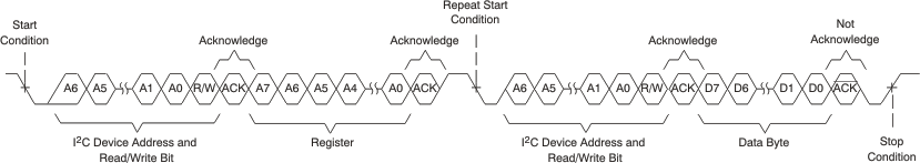 Figure 26. Single-Byte Read Transfer
7.3.6 Multiple-Byte Read
A multiple-byte data-read transfer is identical to a single-byte data-read transfer except that multiple data bytes are transmitted by the TAS2553 to the master device as shown in Figure 27. With the exception of the last data byte, the master device responds with an acknowledge bit after receiving each data byte.
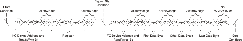 Figure 27. Multiple-Byte Read Transfer
7.3.7 PLL
The TAS2553 has an on-chip PLL to generate the clock frequency for the audio DAC and I-V sensing ADCs. The programmability of the PLL allows operation from a wide variety of clocks that may be available in the system.
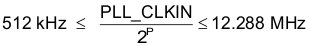
The PLL input supports clocks varying from 512 kHz to 24.576 MHz and is register programmable to enable generation of required sampling rates with fine resolution. Set Register 0x02, D(3) = 1 to activate the PLL. When the PLL is enabled, the PLL output clock PLL_CLK is:

J = 4, 5, 6, … 96
D = 0, 1, 2, ... 9999
P = 0,1
Choose J, D, P such that PLL_CLK = 22.5792 MHz (44.1ksps sampling rate) or 24.5760 MHz (48ksps sampling rate). Program variable J in Register 0x08, D(6:0). Program variable D in Register 0x09, D(5:0) and Register 0x0A, D(7:0). The default value for D is 0. Program variable P in Register 0x08, D(7). The default value for P is 0.
Register 0x01, D(5:4) sets the PLL_CLKIN input to MCLK, BCLK, or IVCLKIN. Set Register 0x01, D(5:4) = 00 to use MCLK, 01 to use BCLK, and 10 to use IVCLKIN.
There is also an option to use a 1.8 MHz internal oscillator for PLL_CLKIN. This is useful for systems using the analog inputs and the I-V sense data returning to a host processor via PDM mode interface. Set Register 0x01, D(5:4) = 11 to use the 1.8 MHz internal oscillator.
To bypass the PLL, set Register 0x09, D(7) = 1. Deactivate the PLL by setting Register 0x02, D(3) = 0.
When the PLL is enabled, the following conditions must be satisfied:
- If D = 0, the PLL clock input (PLL_CLKIN) must satisfy:
- If D ≠ 0, the PLL clock input (PLL_CLKIN) must satisfy:
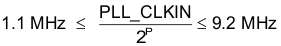
Figure 28 shows the clock distribution tree and the registers required to set the audio input DAC and the I-V sense ADC.
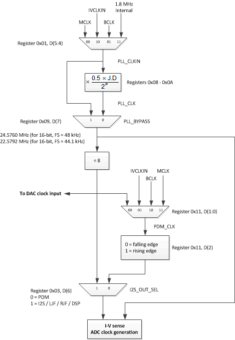 Figure 28. Clock Distribution Tree
7.3.8 Gain Settings
The TAS2553 has one gain register for both analog input and digital input (DAC output) gain. A mux selects only one of these inputs for the Class-D speaker amplifier. The analog and digital inputs cannot be mixed together.
The full-scale DAC output voltage is the same as the maximum analog input voltage (for less than 1% THD): 1 VRMS, or 1.4 VPEAK.
Table 1. TAS2553 Gain Table
| GAIN BYTE: GAIN[4:0] |
NOMINAL GAIN | GAIN BYTE: GAIN[4:0] |
NOMINAL GAIN |
|---|---|---|---|
| 00000 | –7 dB | 10000 | 9 dB |
| 00001 | –6 dB | 10001 | 10 dB |
| 00010 | –5 dB | 10010 | 11 dB |
| 00011 | –4 dB | 10011 | 12 dB |
| 00100 | –3 dB | 10100 | 13 dB |
| 00101 | –2 dB | 10101 | 14 dB |
| 00110 | –1 dB | 10110 | 15 dB |
| 00111 | 0 dB | 10111 | 16 dB |
| 01000 | 1 dB | 11000 | 17 dB |
| 01001 | 2 dB | 11001 | 18 dB |
| 01010 | 3 dB | 11010 | 19 dB |
| 01011 | 4 dB | 11011 | 20 dB |
| 01100 | 5 dB | 11100 | 21 dB |
| 01101 | 6 dB | 11101 | 22 dB |
| 01110 | 7 dB | 11110 | 23 dB |
| 01111 | 8 dB | 11111 | 24 dB |
7.3.9 Class-D Edge Rate Control
The edge rate of the Class-D output is controllable via an I2C register. This allows users the ability to adjust the switching edge rate of the Class-D amplifier, trading off some efficiency for lower EMI. Table 2 lists the typical edge rates.
Table 2. Class-D Edge Rate Control
| ERC BYTE: EDGE[2:0] |
TR AND TF (TYPICAL) |
|---|---|
| 000 | 50 ns |
| 001 | 40 ns |
| 010 | 30 ns |
| 011 | 25 ns |
| 100 | 14 ns |
| 101 | 13 ns |
| 110 | 12 ns |
| 111 | 11 ns |
7.3.10 Battery Tracking AGC
The TAS2553 monitors battery voltage and the audio signal to automatically decrease gain when the battery voltage is low and audio output power is high. This finds the optimal gain to maximize loudness and minimize battery current, providing louder audio and preventing early shutdown at end-of-charge battery voltage levels.
This does not mean the battery tracking AGC automatically decreases amplifier gain when VBAT is below the inflection point. Rather, gain is decreased only when the Class-D output voltage exceeds the limiter level.
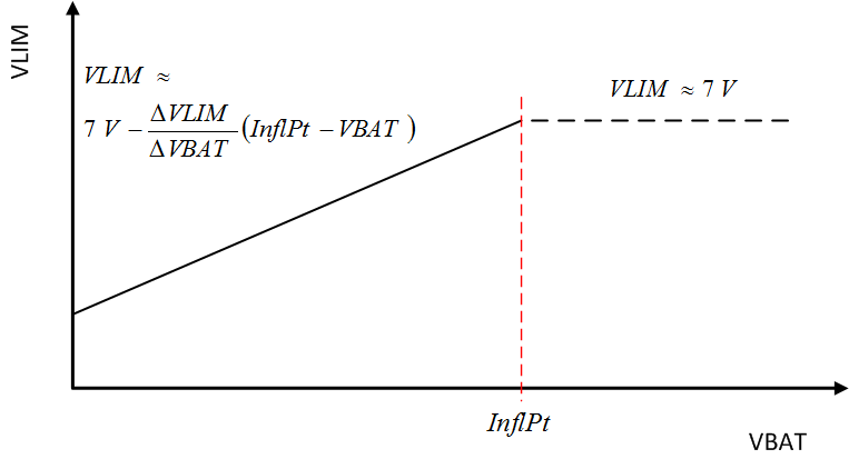 Figure 29. VLIM versus Supply Voltage (VBAT)
When VBAT is greater than the inflection point, VLIM - the peak allowed output voltage - is set by the boost voltage. The inflection point is set in Register 0x0B, Bits 7-0. The inflection point range is 3.0 V to 5.5 V, adjustable in 17.33 mV steps.
When VBAT is less than the inflection point, the peak output voltage is controlled by the slope. Set the VLIM vs. VBAT slope in Register 0x0C, Bits 7-0. This ΔVLIM / ΔVBAT range is 1.2 V/V to 10.75 V/V and is adjustable in 37.3 mV/V steps.
If the audio signal is higher than VLIM, then the gain decreases until the audio signal is just below VLIM. The gain decrease rate (attack time) is set via the I2C interface. If the audio signal is below VLIM and the gain is below the fixed gain, the gain will increase. The gain increase rate (release time) is set via the I2C interface. The attack and release times are selected via I2C interface. Eight attack times are available in 350 µs / dB steps. Sixteen release times are in 105 ms / dB steps. ATK_TIME[2:0] is Register 0x0E, Bits 0-2. REL_TIM[3:0] is Register 0x0F, Bits 3-0.
Table 3. Attack Time Selection
| ATTACK TIME REGISTER BYTE: ATK_TIME[2:0] |
ATTACK TIME ( µS / STEP) |
|---|---|
| 000 | 20 |
| 001 | 370 |
| 010 | 720 |
| 011 | 1070 |
| 100 | 1420 |
| 101 | 1770 |
| 110 | 2120 |
| 111 | 2470 |
Table 4. Release Time Selection
| RELEASE TIME REGISTER BYTE: REL_TIME[3:0] |
RELEASE TIME ( MS / STEP) |
RELEASE TIME REGISTER BYTE: REL_TIME[4:0] |
RELEASE TIME (MS / STEP) |
|---|---|---|---|
| 0000 | 50 | 1000 | 890 |
| 0001 | 155 | 1001 | 995 |
| 0010 | 260 | 1010 | 1100 |
| 0011 | 365 | 1011 | 1205 |
| 0100 | 470 | 1100 | 1310 |
| 0101 | 575 | 1101 | 1415 |
| 0110 | 680 | 1110 | 1520 |
| 0111 | 785 | 1111 | 1625 |
7.4 Device Functional Modes
7.4.1 Audio Digital I/O Interface
Audio data is transferred between the host processor and the TAS2553 via the digital audio data serial interface, or audio bus. The audio bus on this device is very flexible, including left or right-justified data options, support for I2S or PCM protocols, programmable data length options, a TDM mode for multichannel operation, very flexible master/slave configurability for each bus clock line, and the ability to communicate with multiple devices within a system directly.
The audio bus of the TAS2553 can be configured for left or right-justified, I2S, DSP, or TDM modes of operation, where communication with standard telephony PCM interfaces is supported within the TDM mode. These modes are all MSB-first, with data width programmable as 16, 20, 24, or 32 bits by configuring Register 0x05, D(1:0). In addition, the word clock and bit clock can be independently configured in either Master or Slave mode, for flexible connectivity to a wide variety of processors. The word clock is used to define the beginning of a frame, and may be programmed as either a pulse or a square-wave signal. The frequency of this clock corresponds to the maximum of the selected ADC and DAC sampling frequencies.
The bit clock is used to clock in and clock out the digital audio data across the serial bus. This signal can be programmed to generate variable clock pulses by controlling the bit-clock multiply-divide factor in Registers 0x08 through 0x10. The number of bit-clock pulses in a frame may need adjustment to accommodate various word-lengths as well as to support the case when multiple TAS2553 devices may share the same audio bus.
The TAS2553 also includes a feature to offset the position of start of data transfer with respect to the word-clock. This offset is in number of bit-clocks and is programmed in Register 0x06.
To place the DOUT line into a Hi-Z (3-state) condition during all bit clocks when valid data is not being sent, set Register 0x04, D(2) = 1. By combining this capability with the ability to program what bit clock in a frame the audio data begins, time-division multiplexing (TDM) can be accomplished. This enables the use of multiple devices on a single audio serial data bus. When the audio serial data bus is powered down while configured in master mode, the terminals associated with the interface are put into a Hi-Z output state.
7.4.1.1 Right-Justified Mode
Set Register 0x03, D(6) = 0 and Register 0x05, D(3:2) = 10 to place the TAS2553 audio interface into right-justified mode. In right-justified mode, the LSB of the left channel is valid on the rising edge of the bit clock preceding the falling edge of the word clock. Similarly, the LSB of the right channel is valid on the rising edge of the bit clock preceding the rising edge of the word clock.
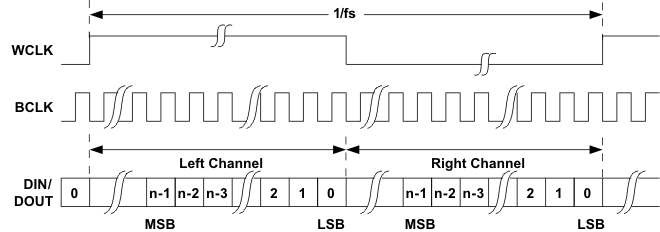 Figure 30. Timing Diagram for Right-Justified Mode
For right-justified mode, the number of bit-clocks per frame should be greater than twice the programmed word-length of the data.
7.4.1.2 Left-Justified Mode
Set Register 0x03, D(7:6) = 01 and Register 0x05, D(3:2) = 11 to place the TAS2553 audio interface into left-justified mode. In left-justified mode, the MSB of the right channel is valid on the rising edge of the bit clock following the falling edge of the word clock. Similarly the MSB of the left channel is valid on the rising edge of the bit clock following the rising edge of the word clock.
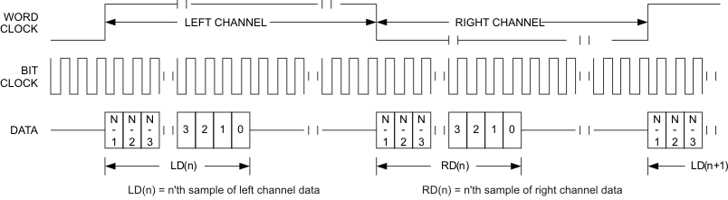 Figure 31. Timing Diagram for Left-Justified Mode
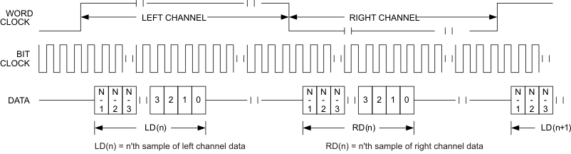 Figure 32. Timing Diagram for Light-Left Mode with Offset=1
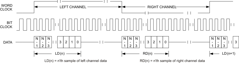 Figure 33. Timing Diagram for Left-Justified Mode with Offset=0 and Inverted Bit Clock
For left-justified mode, the number of bit-clocks per frame should be greater than twice the programmed word-length of the data. Also, the programmed offset value should be less than the number of bit-clocks per frame by at least the programmed word-length of the data.
7.4.1.3 I2S Mode
Set Register 0x03, D(7:6) = 01 and Register 0x05, D(3:2) = 00 to place the TAS2553 audio interface into I2S mode. In I2S mode, the MSB of the left channel is valid on the second rising edge of the bit clock after the falling edge of the word clock. Similarly the MSB of the right channel is valid on the second rising edge of the bit clock after the rising edge of the word clock.
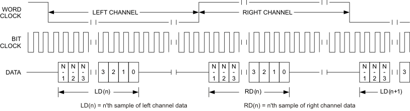 Figure 34. Timing Diagram for I2S Mode
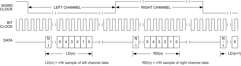 Figure 35. Timing Diagram for I2S Mode with Offset=2
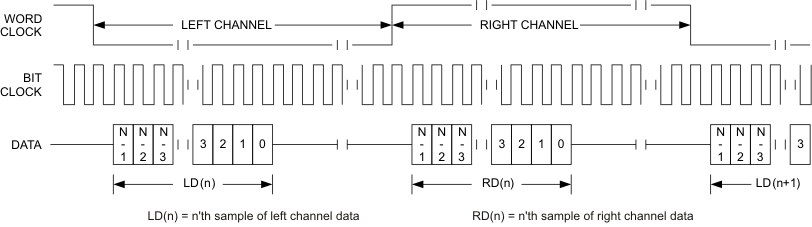 Figure 36. Timing Diagram for I2S Mode with Offset=0 and Inverted Bit Clock
For I2S mode, the number of bit-clocks per channel should be greater than or equal to the programmed word-length of the data. Also the programmed offset value should be less than the number of bit-clocks per frame by at least the programmed word-length of the data.
7.4.1.4 Audio Data Serial Interface Timing (I2S, Left-Justified, Right-Justified Modes)
All specifications at 25°C, IOVDD = 1.8 V
NOTE
All timing specifications are measured at characterization but not tested at final test.
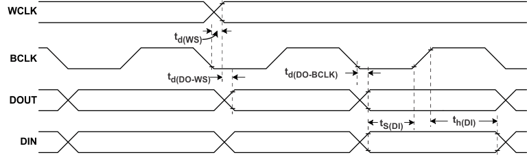 Figure 37. I2S/LJF/RJF Timing in Master Mode
Table 5. I2S/LJF/RJF Timing in Master Mode (see Figure 37)
| PARAMETER | IOVDD=1.8V | IOVDD=3.3V | UNIT | |||
|---|---|---|---|---|---|---|
| MIN | MAX | MIN | MAX | |||
| td(WS) | WCLK delay | 30 | 20 | ns | ||
| td(DO-WS) | WCLK to DOUT delay (For LJF Mode only) | 50 | 25 | ns | ||
| td(DO-BCLK) | BCLK to DOUT delay | 50 | 25 | ns | ||
| ts(DI) | DIN setup | 8 | 8 | ns | ||
| th(DI) | DIN hold | 8 | 8 | ns | ||
| tr | Rise time | 24 | 12 | ns | ||
| tf | Fall time | 24 | 15 | ns | ||
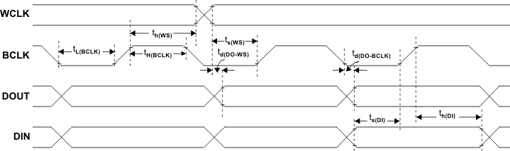 Figure 38. I2S/LJF/RJF Timing in Slave Mode
Table 6. I2S/LJF/RJF Timing in Slave Mode (see Figure 38)
| PARAMETER | IOVDD=1.8V | IOVDD=3.3V | UNIT | |||
|---|---|---|---|---|---|---|
| MIN | MAX | MIN | MAX | |||
| tH(BCLK) | BCLK high period | 35 | 35 | ns | ||
| tL(BCLK) | BCLK low period | 35 | 35 | ns | ||
| ts(WS) | (WS) | 8 | 8 | ns | ||
| th(WS) | WCLK hold | 8 | 8 | ns | ||
| td(DO-WS) | WCLK to DOUT delay (For LJF Mode only) | 50 | 25 | ns | ||
| td(DO-BCLK) | BCLK to DOUT delay | 50 | 25 | ns | ||
| ts(DI) | DIN setup | 8 | 8 | ns | ||
| th(DI) | DIN hold | 8 | 8 | ns | ||
| tr | Rise time | 4 | 4 | ns | ||
| tf | Fall time | 4 | 4 | ns | ||
7.4.1.5 DSP Mode
Set Register 0x03, D(7:6) = 01 and Register 0x05, D(3:2) = 01 to place the TAS2553 audio interface into DSP mode. In DSP mode, the rising edge of the word clock starts the data transfer with the left channel data first and immediately followed by the right channel data. Each data bit is valid on the falling edge of the bit clock.
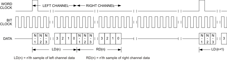 Figure 39. Timing Diagram for DSP Mode
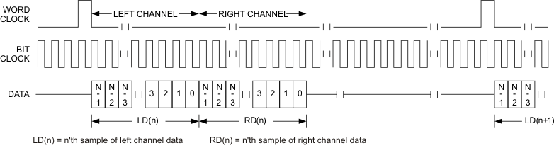 Figure 40. Timing Diagram for DSP Mode with Offset=1
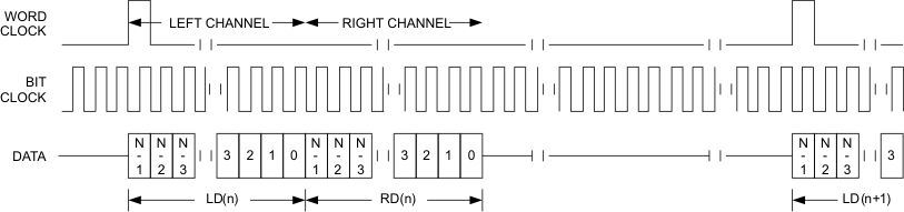 Figure 41. Timing Diagram for DSP Mode with Offset=0 and Inverted Bit Clock
For DSP mode, the number of bit-clocks per frame should be greater than twice the programmed word-length of the data. Also the programmed offset value should be less than the number of bit-clocks per frame by at least the programmed word-length of the data.
7.4.1.6 DSP Timing
All specifications at 25°C, IOVDD = 1.8 V
NOTE
All timing specifications are measured at characterization but not tested at final test.
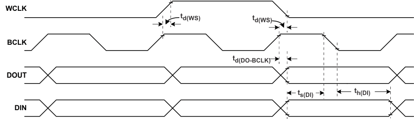 Figure 42. DSP Timing in Master Mode
Table 7. DSP Timing in Master Mode (see Figure 42)
| PARAMETER | IOVDD=1.8V | IOVDD=3.3V | UNIT | |||
|---|---|---|---|---|---|---|
| MIN | MAX | MIN | MAX | |||
| td(WS) | WCLK delay | 30 | 20 | ns | ||
| td(DO-BCLK) | BCLK to DOUT delay | 40 | 20 | ns | ||
| ts(DI) | DIN setup | 8 | 8 | ns | ||
| th(DI) | DIN hold | 8 | 8 | ns | ||
| tr | Rise time | 4 | 4 | ns | ||
| tf | Fall time | 4 | 4 | ns | ||
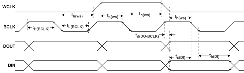 Figure 43. DSP Timing in Slave Mode
Table 8. DSP Timing in Slave Mode (see Figure 43)
| PARAMETER | IOVDD=1.8V | IOVDD=3.3V | UNIT | |||
|---|---|---|---|---|---|---|
| MIN | MAX | MIN | MAX | |||
| tH(BCLK) | BCLK high period | 35 | 35 | ns | ||
| tL(BCLK) | BCLK low period | 35 | 35 | ns | ||
| ts(WS) | (WS) | 8 | 8 | ns | ||
| th(WS) | WCLK hold | 8 | 8 | ns | ||
| td(DO-WS) | WCLK to DOUT delay (For LJF Mode only) | 40 | 22 | ns | ||
| ts(DI) | DIN setup | 8 | 8 | ns | ||
| th(DI) | DIN hold | 8 | 8 | ns | ||
| tr | Rise time | 4 | 4 | ns | ||
| tf | Fall time | 4 | 4 | ns | ||
7.4.2 TDM Mode
Time-division multiplexing (TDM) allows two or more devices to share a common DIN connection and a common DOUT connection. Using TDM mode, all devices transmit their DOUT data in user-specified sub-frames within one WCLK period. When one device transmits its DOUT information, the other devices place their DOUT terminals in a high impedance tri-state mode.
TDM mode is useable with I2S, LJF, RJF, and DSP interface modes. Refer to the respective sections for a description of how to set the TAS2553 into those modes. TDM cannot be used with PDM mode. This is because the PDM requires a continuous stream of samples from one data source.
Use Register 0x06 to set the clock cycle offset from WCLK to the MSB. Each data bit is valid on the falling edge of the bit clock. Set Register 0x04, D(2) = 1 to force DOUT into tri-state when it is not transmitting data. This allows DOUT terminals from multiple TAS2553 devices to share a common wire to the host.
Figure 44. Timing Diagram for I2S in TDM Mode with Offset=2For TDM mode, the number of bit-clocks per frame should be less than the programmed word-length of the data. Also the programmed offset value should be less than the number of bit-clocks per frame by at least the programmed word-length of the data.
Figure 45 shows how to configure the TAS2553 with the TI codec, AIC3254, with both devices sharing DIN and DOUT
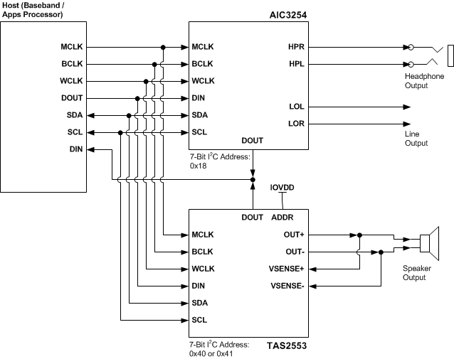 Figure 45. Configuration with TAS2553 and AIC3254 Muxed in TDM Mode
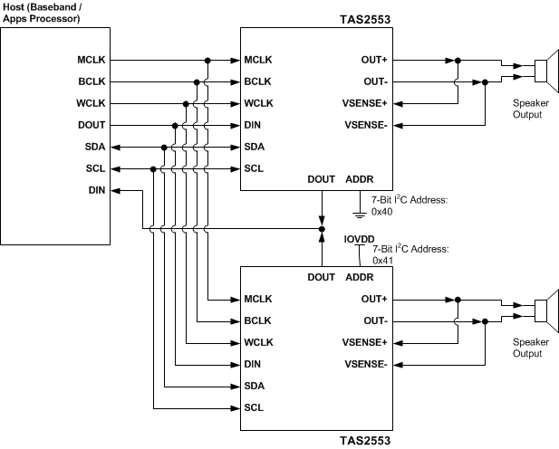 Figure 46. Stereo Configuration with Two TAS2553 DOUT Muxed in TDM Mode
7.4.3 PDM Mode
Set Register 0x03, D(7:6) = 00 to place the TAS2553 audio interface into PDM mode. In PDM mode, the data stream is a continuous stream of undecimated pulse-modulated data that is 64x the sample rate. Because it is a continuous stream, frame synchronization is not required and WCLK is not used. Specifying clocks-per-frame is not required for PDM mode. The PDM input bit clock is IVCLKIN as set in Register 0x11, D(1:0).
The TAS2553 can be configured for I2S input mode and PDM output mode. Figure 47 shows the timing diagram for PDM input mode. Timing specifications are listed in Table 9 and Table 10.
The TAS2553 clocks PDM input data on either the rising edge or falling edge of IVCLKIN as set in Register 0x11, D(2). The device does not read concurrent data on both edges. Set the I2C register to read either rising clock edge or falling clock edge data.
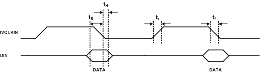 Figure 47. DIN Timing Diagram in PDM Mode, Register 0x11, D(2) = 0
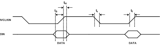 Figure 48. DIN Timing Diagram in PDM Mode, Register 0x11, D(2) = 1
Table 9. PDM Input Timing(2)
| PARAMETER | IOVDD=1.8V(1) | IOVDD=3.3V | UNIT | |||
|---|---|---|---|---|---|---|
| MIN | MAX | MIN | MAX | |||
| ts | DIN setup | 20 | 20 | ns | ||
| th | DIN hold | 3 | 3 | ns | ||
| tr | Rise time | 4 | 4 | ns | ||
| tf | Fall time | 4 | 4 | ns | ||
7.4.3.1 DOUT Timing – PDM Output Mode
Set Register 0x03, D(6) = 0 to transmit PDM data on the DOUT terminal. Register 0x07, D(7:6) selects either I Data, V Data, or both for PDM transmission. Register 0x07, D(5) selects whether the data transmits on either the rising edge or the falling edge of IVCLKIN. The DOUT terminal becomes high-impedance on the opposing clock cycle.
 Figure 49. DOUT Timing in PDM Mode (Data on IVCLKIN High)
 Figure 50. DOUT Timing in PDM Mode (Data on IVCLKIN Low)
Table 10. DOUT Timing in PDM Mode(2)
| PARAMETER | IOVDD=1.8V(1) | IOVDD=3.3V | UNIT | |||
|---|---|---|---|---|---|---|
| MIN | MAX | MIN | MAX | |||
| td(DATA) | IVCLKIN to DOUT delay | 30 | 30 | ns | ||
| td(HI-Z) | IVCLKIN to high impedance state delay | 6 | 6 | ns | ||
7.5 Register Map
The TAS2553 I2C address is 0x40 (7-bit) when ADDR = 0 and 0x41 (7-bit) when ADDR = 1. See the General I2C Operation section for more details.
7.5.1 Register Map Summary
| REGISTER | READ/WRITE | DEFAULT | FUNCTION | |
|---|---|---|---|---|
| DEC | HEX | |||
| 0 | 0x00 | R/W | 0x00 | Device Status Register |
| 1 | 0x01 | R/W | 0x22 | Configuration Register 1 |
| 2 | 0x02 | R/W | 0xFF | Configuration Register 2 |
| 3 | 0x03 | R/W | 0x80 | Configuration Register 3 |
| 4 | 0x04 | R/W | 0x00 | DOUT Tristate Mode |
| 5 | 0x05 | R/W | 0x00 | Serial Interface Control Register 1 |
| 6 | 0x06 | R/W | 0x00 | Serial Interface Control Register 2 |
| 7 | 0x07 | R/W | 0xC0 | Output Data Register |
| 8 | 0x08 | R/W | 0x10 | PLL Control Register 1 |
| 9 | 0x09 | R/W | 0x00 | PLL Control Register 2 |
| 10 | 0x0A | R/W | 0x00 | PLL Control Register 3 |
| 11 | 0x0B | R/W | 0x8F | Battery Tracking Inflection Point Register |
| 12 | 0x0C | R/W | 0x80 | Battery Tracking Slope Control Register |
| 13 | 0x0D | R/W | 0xBE | Limiter Level Control Register |
| 14 | 0x0E | R/W | 0x08 | Limiter Attack Rate and Hysteresis Time |
| 15 | 0x0F | R/W | 0x05 | Limiter Release Rate |
| 16 | 0x10 | R/W | 0x00 | Limiter Integration Count Control |
| 17 | 0x11 | R/W | 0x01 | PDM Configuration Register |
| 18 | 0x12 | R/W | 0x00 | PGA Gain Register |
| 19 | 0x13 | R/W | 0x40 | Class-D Edge Rate Control Register |
| 20 | 0x14 | R/W | 0x00 | Boost Auto-Pass Through Control Register |
| 21 | 0x15 | R/W | 0x00 | Reserved |
| 22 | 0x16 | R | 0x00 | Version Number |
| 23 | 0x17 | R/W | 0x00 | Reserved |
| 24 | 0x18 | R | 0x00 | Reserved |
| 25 | 0x19 | R | 0x00 | VBAT Data Register |
7.5.2 Register 0x00: Device Status Register
This register uses latched faults. The fault bits are clear on write. Read-only commands retain the latched value of the fault bit.
| BIT | NAME | READ/WRITE | DEFAULT | DESCRIPTION |
|---|---|---|---|---|
| 7-6 | R/W | 00 | Reserved. Write only default values. | |
| 5 | PLL_OUT_OF_LOCK | R/W | 0 | PLL lock 0 = PLL is locked 1 = PLL is not locked |
| 4-2 | R/W | 0 | Reserved. Write only default values. | |
| 1 | CLASSD_ILIM | R/W | 0 | Class-D over-current 0 = Normal operation 1 = Class-D output current limit has been exceeded |
| 0 | THERMAL | R/W | 0 | Thermal limit 0 = Normal operation 1 = Limit exceeded |
7.5.3 Register 0x01: Configuration Register 1
| BIT | NAME | READ/WRITE | DEFAULT | DESCRIPTION |
|---|---|---|---|---|
| 7-6 | R/W | 00 | Reserved. Write only default values. | |
| 5-4 | PLL_SRC | R/W | 10 | PLL Input 00 = MCLK 01 = BCLK 10 = IVCLKIN 11 = 1.8 MHz fixed internal oscillator |
| 3 | R/W | 0 | Reserved. Write only default values. | |
| 2 | MUTE | R/W | 0 | Triggers mute of Class-D channel controller. 0 = Not muted 1 = Muted |
| 1 | SWS | R/W | 1 | Software shutdown. When high shuts down all blocks and places part in low power mode. THIS BIT MUST BE SET TO ZERO ONLY AFTER THE DEVICE CONFIGURATION IS COMPLETE. |
| 0 | DEV_RESET | R/W | 0 | Synchronous reset of all digital registers & control circuitry. |
7.5.4 Register 0x02: Configuration Register 2
| BIT | NAME | READ/WRITE | DEFAULT | DESCRIPTION |
|---|---|---|---|---|
| 7 | CLASSD_EN | R/W | 1 | Class D Enable |
| 6 | BOOST_EN | R/W | 1 | Boost Enable |
| 5 | APT_EN | R/W | 1 | Auto Pass-Thru Enable |
| 4 | RESERVED | R/W | 0 | Reserved. Write only default values. |
| 3 | PLL_EN | R/W | 1 | PLL Enable |
| 2 | LIM_EN | R/W | 1 | Battery Tracking AGC Enable |
| 1 | IVSENSE_EN | R/W | 1 | I/V Sense Enable |
| 0 | RESERVED | R/W | 1(1) | Reserved. MUST BE WRITTEN TO ZERO DURING CONFIGURATION SEQUENCE as shown in Initialization. |
7.5.5 Register 0x03: Configuration Register 3
| BIT | NAME | READ / WRITE | DEFAULT | DESCRIPTION |
|---|---|---|---|---|
| 7 | ANALOG_IN_SEL | R/W | 1 | Selects analog in path for data to class-D. When set to zero (digital in), no signal should be present on the analog terminals. 0 = Digital Audio Input 1 = Analog Audio Input |
| 6 | I2S_OUT_SEL | R/W | 0 | Selects between PDM and I2S for I/V Sense output data format. 0 = PDM 1 = I2S |
| 5 | PDM_IN_SEL | R/W | 0 | Selects PDM as input to modulator 0 = PDM is not selected 1 = PDM is selected only if Digital Audio Input is selected (Reg 0x03 D[7] = 0) |
| 4-3 | DIN_SOURCE_SEL | R/W | 00 | DIN Source Select 00 = Modulator input muted 01 = Use left stream for modulator 10 = Use right stream for modulator 11 = Use average of left and right streams for modulator |
| 2-0 | WCLK_FREQ | R/W | 000 | WCLK Frequency 000 = 8 kHz 001 = 11.025 kHz / 12 kHz 010 = 16 kHz 011 = 22.05 kHz / 24 kHz 100 = 32 kHz 101 = 44.1 kHz / 48 kHz 110 = 88.2 kHz / 96 kHz 111 = 176.4 kHz / 192 kHz |
7.5.6 Register 0x04: DOUT Tristate Mode
For systems with multiple devices sharing a common DOUT line with a TDM interface mode, set Bit 2 to 1 to ensure DOUT stays in high-impedance tri-state mode when it is not transmitting data.
| BIT | NAME | READ / WRITE | DEFAULT | DESCRIPTION |
|---|---|---|---|---|
| 7-3 | R/W | 0000 0 | Reserved. Write only default values. | |
| 2 | SDOUT_TRISTATE | R/W | 0 | DOUT Tri-state Mode (for I2S mode only, see Reg 0x03, bit 7) 0 = DOUT set to logic low when not transmitting data 1 = DOUT in tristate when not transmitting data |
| 1-0 | R/W | 00 | Reserved. Write only default values. |
7.5.7 Register 0x05: Serial Interface Control Register 1
| BIT | NAME | READ/WRITE | DEFAULT | DESCRIPTION |
|---|---|---|---|---|
| 7 | WCLKDIR | R/W | 0 | WCLK Direction 0 = WCLK is an input terminal 1 = WCLK is an output terminal |
| 6 | BCLKDIR | R/W | 0 | BCLK Direction 0 = BCLK is an input terminal 1 = BCLK is an output terminal |
| 5-4 | CLKSPERFRAME | R/W | 00 | Clocks per Frame 00 = 32 clocks 01 = 64 clocks 10 = 128 clocks 11 = 256 clocks |
| 3-2 | DATAFORMAT | R/W | 00 | Data Format 00 = I2S format 01 = DSP (PCM format) 10 = Right justified format (RJF) 11 = Left justified format (LJF) |
| 1-0 | WORDLENGTH | R/W | 00 | Word Length 00 = 16 bits 01 = 20 bits 10 = 24 bits 11 = 32 bits |
7.5.8 Register 0x06: Serial Interface Control Register 2
This register sets the clock cycle offset between the WCLK edge to the MSB of serial interface patterns. This is useful for TDM mode where multiple devices share DIN or DOUT lines.
| BIT | NAME | READ / WRITE | DEFAULT | DESCRIPTION |
|---|---|---|---|---|
| 7-0 | I2S_SHIFT_REG | R/W | 0000 0000 | Offset from WCLK to MSB in serial interface patterns. 0000 0000 = 0 bit offset 0000 0001 = 1 bit offset …. 1111 1111 = 255 bit offset |
7.5.9 Register 0x07: Output Data Register
This register sets the output data for DOUT. Most systems will simply set L_DATA_OUT to transmit output current data and R_DATA_OUT to transmit voltage data. Other data is available, like VBAT voltage, VBOOST voltage, and PGA gain.
Bit 5 is a dual-purpose bit. If I2S_OUT_SEL = 0 (Register 0x03, Bit 6) and the PDM_DATA_SEL bits are set to transmit only I-Data or V-Data, then Bit 5 dictates if that data is transmitted on the clock rising edge or falling edge. This allows two TAS2553 devices in PDM mode to tie their DOUT lines together and connect to the host digital mic input. In this configuration, each device broadcasts its output current or output voltage information – one on the rising edge of the clock, the other on the falling edge. This is a simple interface technique that does not require programming the host for TDM-interface mode.
| BIT | NAME | READ / WRITE | DEFAULT | DESCRIPTION |
|---|---|---|---|---|
| 7-6 | PDM_DATA_SEL | R/W | 11 | PDM Data Select These bits are operative only if I2S_OUT_SEL = 0 for PDM mode (see Register 0x03, Bit 6). 00 - I Data Only - Select Ch1 or Ch2 with bit[5] 01 - V Data Only - Select Ch1 or Ch2 with bit[5] 10 - I/V Data (Ch1/2) 11 - V/I Data (Ch1/2) |
| 5-3 | R_DATA_OUT | R/W | 000 | Serial Interface Data, Right Channel Bit 5 is a dual-purpose bit, depending on the state of I2S_OUT_SEL (Register 0x03, Bit 6). If I2S_OUT_SEL = 0 and PDM_DATA_SEL = 00 or 01 (for single-channel PDM output mode), then Bit 5 will select whether data is transmitted on the rising or falling edge of the clock. 0xx = Falling Edge (Ch 1) 1xx = Rising Edge (Ch 2) If I2S_OUT_SEL = 1, then Bits 5-3 have the same function as L_DATA_OUT. Read the description in L_DATA_OUT for requirements on BCLK and WORD_LENGTH. 000 = I Data (16'b) 001 = V Data (16'b) 010 = VBAT Data (8'b) 011 = VBOOST Data (8'b) 100 = PGA Gain (5'b) 101 = I Data, V Data (32'b) 110 = VBAT, VBOOST, PGA Gain (21'b) 111 = Disabled (Hi-Z) NOTE: For VBAT and VBOOST, the device must be in a mode that uses this information, such as Battery Tracking AGC. |
| 2-0 | L_DATA_OUT | R/W | 000 | Serial Interface Data, Left Channel Users must provide enough BCLK cycles per WCLK frame to shift all the data out. If there are additional BCLK cycles per WCLK frame beyond the WORD_LENGTH setting, the data line will be HI-Z if SDOUT_TRISTATE (Register 0x04, Bit 3) is set to 1; otherwise the data line will be held low for the extra BCLK cycles. Users must also program a sufficient WORD_LENGTH setting. If selected data contains fewer bits than WORD_LENGTH setting, the extra bits will be 0's. 000 = I Data (16'b) 001 = V Data (16'b) 010 = VBAT Data (8'b) 011 = VBOOST Data (8'b) 100 = PGA Gain (5'b) 101 = I Data, V Data (32'b) 110 = VBAT, VBOOST, PGA Gain (21'b) 111 = Disabled (Hi-Z) NOTE: For VBAT and VBOOST, the device must be in a mode that uses this information, such as Battery Tracking AGC. |
7.5.10 Register 0x08: PLL Control Register 1
The equation for the PLL frequency is:
J = 4, 5, 6, … 96
D = 0, 1, 2, ... 9999
P = 0,1
Registers 0x08 – 0x0A will only update when the PLL is disabled. To update the J, D, and P coefficients, set PLL_EN = 0 (Register 0x02, Bit 3) to disable the PLL, update Registers 0x08 – 0x0A, then set PLL_EN = 1 to activate the PLL.
| BIT | NAME | READ / WRITE | DEFAULT | DESCRIPTION |
|---|---|---|---|---|
| 7 | PLL_PRESCALE_SEL | R/W | 0 | PLL P Pre-Scale Select 1: P = 1 0: P = 0 |
| 6-0 | PLL_J | R/W | 001 0000 | PLL J Characteristic Multiplier Value 000 0000 … 000 0011: Do not use 000 0100: J=4 … 001 0000: J=16 … 101 1111: J=95 110 0000: J=96 110 0001 ... 111 1111: Do not use |
7.5.11 Register 0x09: PLL Control Register 2
| BIT | NAME | READ / WRITE | DEFAULT | DESCRIPTION |
|---|---|---|---|---|
| 7 | PLL_BYPASS | R/W | 0 | 1: Bypasses PLL by setting PLL_CLK = PLL_CLKIN 0: Sets PLL_CLK according to Equation 2 |
| 6 | 0 | Reserved | ||
| 5-0 | PLL_D[13:8] | R/W | 00 0000 | PLL D Mantissa Multiplier Value (LSB) The complete PLL D value comprises PLL_D[13:8] (MSB) concatenated with PLLD[7:0] (LSB) 00 0000 0000 0000: D=0000 00 0000 0000 0001: D=0001 … 10 0111 0000 1110: D=9998 10 0111 0000 1111: D=9999 10 0111 0001 0000 ... 11 1111 1111 1111: Do not use |
7.5.12 Register 0x0A: PLL Control Register 3
| BIT | NAME | READ / WRITE | DEFAULT | DESCRIPTION |
|---|---|---|---|---|
| 7-0 | PLL_D[7:0] | R/W | 0000 0000 | PLL D Mantissa Multiplier Value (LSB) The complete PLL D value comprises PLL_D[13:8] (MSB) concatenated with PLLD[7:0] (LSB) 00 0000 0000 0000: D=0000 00 0000 0000 0001: D=0001 … 10 0111 0000 1110: D=9998 10 0111 0000 1111: D=9999 10 0111 0001 0000 ... 11 1111 1111 1111: Do not use |
7.5.13 Register 0x0B: Battery Tracking Inflection Point Register
| BIT | NAME | READ / WRITE | DEFAULT | DESCRIPTION |
|---|---|---|---|---|
| 7-0 | INFLECTION | R/W | 1000 1111 | Battery Inflection Point Value 0.01733 V per step 0000 0000 = RESERVED … 0110 1100 = RESERVED 0110 1101 = 3.00 V … 1111 1101 = 5.49 V 1111 1110 = 5.50 V 1111 1111 = RESERVED |
7.5.14 Register 0x0C: Battery Tracking Slope Control Register
| BIT | NAME | READ / WRITE | DEFAULT | DESCRIPTION |
|---|---|---|---|---|
| 7-0 | SLOPE | R/W | 1000 0000 | Battery Tracking Slope Value (ΔVLIM / ΔVBAT) 0.0373 V/V per step 0000 0000 = 1.2 V/V 0000 0001 = 1.237 V/V … 1111 1101 = 10.675 V/V 1111 1110 = 10.713 V/V 1111 1111 = 10.75 V/V |
7.5.15 Register 0x0D: Reserved Register
| BIT | NAME | READ / WRITE | DEFAULT | DESCRIPTION |
|---|---|---|---|---|
| 7-0 | R/W | 1011 1110 | Write to 0xA9 during initialization. See Initialization. |
7.5.16 Register 0x0E: Battery Tracking Limiter Attack Rate and Hysteresis Time
| BIT | NAME | READ / WRITE | DEFAULT | DESCRIPTION |
|---|---|---|---|---|
| 7-6 | HYSTERESIS | R/W | 00 | Hysteresis before re-arming release time 00 = No hysteresis 01 = 4.36 mV hysteresis 10 = 13.08 mV hysteresis 11 = 30.52 mV hysteresis |
| 5 | R/W | 0 | Write to 1 during initialization. See Initialization. | |
| 4-3 | APT_DIS_VOLTAGE | R/W | 01 | VBAT threshold below which Boost APT is disabled and the boost remains active regardless of Class-D output voltage. 00 = 2.5 V 01 = 2.7 V 10 = 2.9 V 11 = 3.1 V |
| 2-0 | ATTACK_TIME | R/W | 000 | Attack Time 350 µs / dB per step 000 = 20 µs / dB 001 = 370 µs / dB … 110 = 2120 µs / dB 111 = 2470 µs / dB |
7.5.17 Register 0x0F: Battery Tracking Limiter Release Rate
| BIT | NAME | READ / WRITE | DEFAULT | DESCRIPTION |
|---|---|---|---|---|
| 7-4 | R/W | 00 | Reserved. Write only default values. | |
| 3-0 | REL_TIME | R/W | 0100 | Release Time 105 ms / dB per step 0000 = 50 ms / dB 0001 = 155 ms / dB … 1110 = 1520 ms / dB 1111 = 1625 ms / dB |
7.5.18 Register 0x10: Battery Tracking Limiter Integration Count Control
Limiter integration affects how the AGC state machine interprets the AGC output voltage trigger threshold. Increasing the integration count requires more AGC output peaks to exceed the limiter threshold before the limiter changes its gain.
| BIT | NAME | READ / WRITE | DEFAULT | DESCRIPTION |
|---|---|---|---|---|
| 7-6 | UP_DWN_RATIO | R/W | 00 | Control Integration Count Up/Down Ratio The UP_DWN_RATIO sets the ratio of the addition to and the subtraction from the integration count, meaning that the input has to be below the limit threshold for 4UP_DWN_RATIO counts before the integration count is reduced. |
| 5-0 | INT_CNT | R/W | 00 0000 | Integration Count Control Register Larger values increase filtering before the attack and decay time are triggered. |
7.5.19 Register 0x11: PDM Configuration Register
Sets the PDM clock source and whether channel 1 data is transmitted on the rising or falling edge of the clock. Channel 2 transmits on the opposite edge.
| BIT | NAME | READ / WRITE | DEFAULT | DESCRIPTION |
|---|---|---|---|---|
| 7-3 | R/W | 0 0000 | Reserved. Write only default values. | |
| 2 | PDM_DATA_ES | R/W | 0 | PDM Data Edge Select 0 = falling edge 1 = rising edge |
| 1-0 | PDM_CLK_SEL | R/W | 01 | PDM Clock Select 00 = PLL / 8 01 = IVCLKIN 10 = BCLK 11 = MCLK |
7.5.20 Register 0x12: PGA Gain Register
| BIT | NAME | READ / WRITE | DEFAULT | DESCRIPTION |
|---|---|---|---|---|
| 7-5 | R/W | 000 | Reserved. Write only default values. | |
| 4-0 | PGA_GAIN | R/W | 0 0000 | PGA Gain Value 00000 = -7 dB 00001 = -6 dB … 11110 = +23 dB 11111 = +24 dB |
7.5.21 Register 0x13: Class-D Edge Rate Control Register
| BIT | NAME | READ / WRITE | DEFAULT | DESCRIPTION |
|---|---|---|---|---|
| 7 | GAINCOMP_EN | R/W | 0 | I-V Sense Gain Compensation Control Enables AGC compensation for current sense feedback. AGC compensation increases the gain of the current sense data by the same gain the AGC instantaneously attenuates. 0 = No I-V sense gain compensation 1 = Gain compensation enabled |
| 6-4 | ERC_SEL | R/W | 100 | Class-D Output Edge Rate Control 000 = 50 ns 001 = 40 ns 010 = 29 ns 011 = 25 ns 100 = 14 ns (default) 101 = 13 ns 110 = 12 ns 111 = 11 ns |
| 3-0 | R/W | 0000 | Reserved. Write only default values. |
7.5.22 Register 0x14: Boost Auto-Pass Through Control Register
Auto-Pass Through deactivates the boost converter when the battery voltage is sufficient for the required Class-D output voltage. This register sets the threshold for activating the boost converter and the delay time between the Class-D output voltage dropping below the threshold before the boost converter deactivates.
| BIT | NAME | READ / WRITE | DEFAULT | DESCRIPTION |
|---|---|---|---|---|
| 7-4 | R/W | 0000 | Reserved. Write only default values. | |
| 3-2 | APT_THRESHOLD | R/W | 00 | Analog Input – Auto-Pass Through Threshold The boost converter activates when the Class-D output voltage exceeds this threshold voltage. 00 = 0.5 V 01 = 1.0 V 10 = 1.4 V 11 = 2.0 V Digital Input – Auto-Pass Through Threshold The boost converter activates when the Class-D output voltage exceeds this threshold voltage. 00 = 0.2 V 01 = 0.7 V 10 = 1.1 V 11 = 1.7 V |
| 1-0 | APT_DELAY_SEL | R/W | 00 | Auto-Pass Thru Delay The delay between the Class-D output voltage dropping below the auto-pass thru threshold voltage and the boost converter deactivating. 00 = 50 ms 01 = 75 ms 10 = 125 ms 11 = 200 ms |
7.5.23 Register 0x15: Reserved Register
| BIT | NAME | READ / WRITE | DEFAULT | DESCRIPTION |
|---|---|---|---|---|
| 7-0 | R | 0000 0000 | Reserved |
7.5.24 Register 0x16: Version Number
7.5.25 Register 0x17: Reserved Register
| BIT | NAME | READ / WRITE | DEFAULT | DESCRIPTION |
|---|---|---|---|---|
| 7-0 | R | 0000 0000 | Reserved |
7.5.26 Register 0x18: Reserved Register
| BIT | NAME | READ / WRITE | DEFAULT | DESCRIPTION |
|---|---|---|---|---|
| 7-0 | R | 0000 0000 | Reserved |
7.5.27 Register 0x19: VBAT Data Register
| BIT | NAME | READ / WRITE | DEFAULT | DESCRIPTION |
|---|---|---|---|---|
| 7-0 | VBAT | R | 0000 0000 | Battery Voltage Data VBAT data is only available when the device is in a mode that uses the VBAT measurement, such as Battery Tracking AGC. 1 LSB ≈ 17.33 mV 0000 0000 = RESERVED ... 0100 1001 = RESERVED 0101 0000 = 2.5 V … 1111 1111 = 5.55 V |