SLAS978B September 2013 – February 2014 TAS2553
PRODUCTION DATA.
- 1 Features
- 2 Applications
- 3 Description
- 4 Revision History
- 5 Terminal Configuration and Functions
- 6 Specifications
-
7 Detailed Description
- 7.1 Overview
- 7.2 Functional Block Diagram
- 7.3 Feature Description
- 7.4 Device Functional Modes
- 7.5
Register Map
- 7.5.1 Register Map Summary
- 7.5.2 Register 0x00: Device Status Register
- 7.5.3 Register 0x01: Configuration Register 1
- 7.5.4 Register 0x02: Configuration Register 2
- 7.5.5 Register 0x03: Configuration Register 3
- 7.5.6 Register 0x04: DOUT Tristate Mode
- 7.5.7 Register 0x05: Serial Interface Control Register 1
- 7.5.8 Register 0x06: Serial Interface Control Register 2
- 7.5.9 Register 0x07: Output Data Register
- 7.5.10 Register 0x08: PLL Control Register 1
- 7.5.11 Register 0x09: PLL Control Register 2
- 7.5.12 Register 0x0A: PLL Control Register 3
- 7.5.13 Register 0x0B: Battery Tracking Inflection Point Register
- 7.5.14 Register 0x0C: Battery Tracking Slope Control Register
- 7.5.15 Register 0x0D: Reserved Register
- 7.5.16 Register 0x0E: Battery Tracking Limiter Attack Rate and Hysteresis Time
- 7.5.17 Register 0x0F: Battery Tracking Limiter Release Rate
- 7.5.18 Register 0x10: Battery Tracking Limiter Integration Count Control
- 7.5.19 Register 0x11: PDM Configuration Register
- 7.5.20 Register 0x12: PGA Gain Register
- 7.5.21 Register 0x13: Class-D Edge Rate Control Register
- 7.5.22 Register 0x14: Boost Auto-Pass Through Control Register
- 7.5.23 Register 0x15: Reserved Register
- 7.5.24 Register 0x16: Version Number
- 7.5.25 Register 0x17: Reserved Register
- 7.5.26 Register 0x18: Reserved Register
- 7.5.27 Register 0x19: VBAT Data Register
- 8 Applications and Implementation
- 9 Power Supply Recommendations
- 10Layout
- 11Device and Documentation Support
- 12Mechanical, Packaging, and Orderable Information
Package Options
Mechanical Data (Package|Pins)
- YFF|30
Thermal pad, mechanical data (Package|Pins)
Orderable Information
6 Specifications
6.1 Absolute Maximum Ratings
over operating free-air temperature range, TA = 25°C (unless otherwise noted)| MIN | MAX | UNIT | ||
|---|---|---|---|---|
| VBAT | Battery voltage | –0.3 | 6.0 | V |
| AVDD | Analog supply voltage | –0.3 | 2.5 | V |
| IOVDD | I/O Supply voltage | –0.3 | 3.9 | V |
| AIN+, AIN– | Analog input voltage | –0.3 | AVDD + 0.3 | V |
| Digital input voltage | –0.3 | IOVDD + 0.3 | V | |
| Output continuous total power dissipation | See Thermal Information | NA | ||
6.2 Handling Ratings
| PARAMETER | DEFINITION | MIN | MAX | UNIT |
|---|---|---|---|---|
| Tstg | Storage temperature range | –65 | 150 | °C |
| ESD | HBM | 3000 | V | |
| CDM | 1500 |
6.3 Recommended Operating Conditions
over operating free-air temperature range (unless otherwise noted)| MIN | NOM | MAX | UNIT | ||
|---|---|---|---|---|---|
| VBAT | Battery voltage | 3.0 | 5.5 | V | |
| AVDD | Analog supply voltage | 1.65 | 1.8 | 1.95 | V |
| IOVDD | I/O supply voltage | 1.5 | 1.8 | 3.6 | V |
| TA | Operating free-air temperature | –40 | 85 | °C | |
| TJ | Operating junction temperature | –40 | 150 | °C |
6.4 Thermal Information
| THERMAL METRIC(1) | TAS2553 | UNIT | |
|---|---|---|---|
| YFF (30 TERMINALS) | |||
| θJA | Junction-to-ambient thermal resistance | 76.5 | °C/W |
| θJCtop | Junction-to-case (top) thermal resistance | 0.2 | |
| θJB | Junction-to-board thermal resistance | 44.0 | |
| ψJT | Junction-to-top characterization parameter | 1.6 | |
| ψJB | Junction-to-board characterization parameter | 43.4 | |
(1) For more information about traditional and new thermal metrics, see the IC Package Thermal Metrics application report, SPRA953.
6.5 Electrical Characteristics
VBAT = 3.6 V, AVDD = IOVDD = 1.8 V, EN = IOVDD, SWS = 0, Gain = 15 dB, ERC = 14 ns, RL = 8 Ω + 33 µH, 48 kHz sample rate for digital input (unless otherwise noted)| PARAMETER | TEST CONDITIONS | MIN | TYP | MAX | UNIT | |
|---|---|---|---|---|---|---|
| BOOST CONVERTER | ||||||
| Boost Output Voltage | Average voltage (w/o including ripple). Includes load regulation (0-0.6A) and line regulation (VBAT = 3.0 – 4.8V). | 7.5 | V | |||
| Boost Converter Switching Frequency | 1.8 | MHz | ||||
| CLASS-D CHANNEL | ||||||
| Max Analog Input | For THD+N < 1% | 1 | VRMS | |||
| Full-Scale DAC Output | All digital interface modes | 1 | VRMS | |||
| Load Resistance (Load Spec Reisistance) | 6 | 8 | Ω | |||
| Class-D Frequency | 764 | kHz | ||||
| Class-D + Boost Efficiency | VBAT = 3.0 – 4.8 V, Pout = 1 W (sinewave) | 67% | ||||
| Class-D Output Current Limit (Short Circuit Protection) | VBOOST = 7.5 V, OUT– shorted to VBAT or VBOOST | 3.7 | A | |||
| Class-D Output Offset Voltage in Analog Input Mode | VBAT = 3.6 V, AV = 15 dB, RL = 8 Ω, input shorted to ground through single capacitor | -7.4 | 4.6 | mV | ||
| Class-D Output Offset Voltage in Digital Input Mode | VBAT = 3.6 V, AV = 15 dB, RL =8 Ω, 0's data | -9.8 | 5.6 | mV | ||
| Programmable Channel Gain Range (PGA + class-D), minimum | Typical value, analog and digital input | -7 | dB | |||
| Programmable Channel Gain Range (PGA + class-D), maximum | Typical value, analog and digital input | 24 | dB | |||
| Programmable Channel Gain Step (PGA + class-D) | Typical value, analog and digital input | 1 | dB | |||
| Mute Attenuation | Device in shutdown, digital input only | 103 | dB | |||
| VBAT Power Supply Rejection Ratio (PSRR) | Ripple of 200mVpp @ 217 Hz, Gain = 15 dB, analog and digital input | 63 | dB | |||
| Ripple of 200mVpp @ 1 kHz, Gain = 15 dB, analog and digital input | 60 | |||||
| Ripple of 200mVpp @ 4 kHz, Gain = 15 dB, analog and digital input | 60 | |||||
| AVDD Power Supply Rejection Ratio (PSRR) | Ripple of 200mVpp @ 217 Hz, Gain = 15 dB, analog and digital input | 69 | dB | |||
| Ripple of 200mVpp @ 1 kHz, Gain = 15 dB, analog and digital input | 67 | |||||
| Ripple of 200mVpp @ 4 kHz, Gain = 15 dB, analog and digital input | 62 | |||||
| Common Mode Rejection Ratio | Ripple of 200mVpp @ 217 Hz, Gain = 15 dB, analog input | 59 | dB | |||
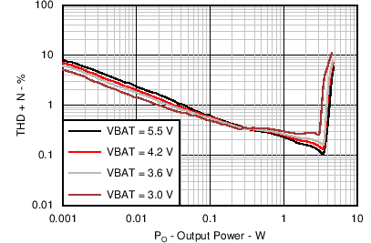
| THD+N | 1 kHz, Po = 0.1W, VBAT = 3.6 V, RL = 8 Ω |
0.6% | ||||
| 1 kHz, Po = 0.5W, VBAT = 3.6 V, RL = 8 Ω |
0.7% | |||||
| 1 kHz, Po = 1 W, VBAT = 3.6 V, RL = 8 Ω | 0.9% | |||||
| 1 kHz, Po = 2 W, VBAT = 3.6 V, RL = 8 Ω | 1.3% | |||||
| Output Integrated Noise (20Hz-20kHz) - 8Ω | A-wt Filter, Gain = 15 dB, DAC modulator switching | 131% | µV | |||
| A-wt Filter, Gain = 15 dB, Analog In, Inputs shorted | 173% | |||||
| Max Output Power, 8-Ω Load | THD+N = 1%, VBAT = 3.0 V | 2.8 | W | |||
| THD+N = 1%, VBAT = 3.6 V | 2.8 | |||||
| Output Impedance in Shutdown | EN = 0 V | 10 | kΩ | |||
| Startup Time | Analog/digital input measured from time when device is taken out of software shutdown | 8 | mS | |||
| Shutdown Time | Measured from time when device is programmed in software shutdown mode | 1 | µS | |||
| INPUT SECTION | ||||||
| Full-scale DAC output | All digital interface modes | 1.0 | VRMS | |||
| Maximum analog input voltage | 1.0 | VRMS | ||||
| RIN | Input impedance (terminals AIN+, AIN-) | EN = IOVDD, Amplifier active | 10 | kΩ | ||
| EN = 0 V, In shutdown | 19 | |||||
| CURRENT SENSE | ||||||
| Current Sense Full Scale | Peak current which will give full scale digital output | 1.4 | APEAK | |||
| Current Sense Accuracy | IOUT = 354 mARMS (1 W) | 1% | ||||
| Current Sense Offset | Input referred | 0.0029 | mA | |||
| Current Sense Gain Error | 0.09 | dB | ||||
| THD+N | Distortion + Noise | Po = 1.0W (Load = 8Ω + 33 µH) | 0.17% | |||
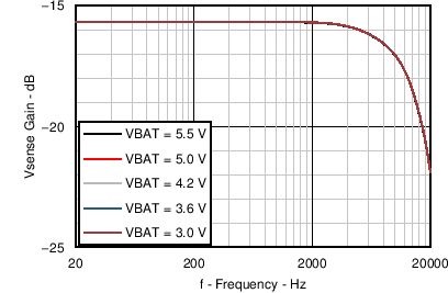
| VOLTAGE SENSE | ||||||
| Voltage Sense Full Scale | Peak voltage which will give full scale digital output | 8.5 | VPEAK | |||
| Voltage Sense Accuracy | VOUT = 2.83 Vrms (1W) | 2.2% | ||||
| Voltage Sense Offset | Input referred | 1.45 | mV | |||
| Voltage Sense Gain Error | -0.20 | dB | ||||
| THD+N | Distortion + Noise | Po = 1.0 W (Load = 8Ω + 33μH) | 0.08% | |||
| INTERFACE | ||||||
| FMCLK | MCLK frequency | 0.512 | 49.15 | MHz | ||
| FPDM | PDM Clock (IVCLK) Frequency Range | 1.636 | 3.25 | MHz | ||
| PDMDC | PDM Clock (IVCLK) Duty Cycle Range | 40% | 60% | |||
| POWER CONSUMPTION | ||||||
| Power Consumption with Analog Input and IV Sense Disabled | From VBAT, PLL off, no signal | 7.10 | mA | |||
| From AVDD, PLL off, no signal | 3.73 | mA | ||||
| From IOVDD, PLL off, no signal | 0.04 | mA | ||||
| Power Consumption with Digital Input and IV Sense Disabled | From VBAT, PLL off, no signal | 7.31 | mA | |||
| From AVDD, PLL off, no signal | 4.05 | mA | ||||
| From IOVDD, PLL off, no signal | 0.32 | mA | ||||
| Power Consumption with Analog Input and IV Sense Enabled | From VBAT, PLL on, no signal | 5.84 | mA | |||
| From AVDD, PLL on, no signal | 7.10 | mA | ||||
| From IOVDD, PLL on, no signal | 0.32 | mA | ||||
| Power Consumption with Digital Input and IV Sense Enabled | From VBAT, PLL on, no signal | 7.32 | mA | |||
| From AVDD, PLL on, no signal | 8.03 | mA | ||||
| From IOVDD, PLL on, no signal | 0.32 | mA | ||||
| Power Consumption in Hardware Shutdown | From VBAT, EN = 0 | 0.1 | µA | |||
| From AVDD, EN = 0 | 0.2 | µA | ||||
| From IOVDD, EN = 0 | 0.0 | µA | ||||
| Power Consumption in Software Shutdown | From VBAT | 11.4 | µA | |||
| From AVDD | 9.1 | µA | ||||
| From IOVDD | 130 | µA | ||||
| DIGITAL INPUT / OUTPUT | ||||||
| VIH | High-level digital input voltage | 0.7 x IOVDD | V | |||
| VIL | Low-level digital input voltage | 0.3 x IOVDD | V | |||
| VOH | High-level digital output voltage | 0.9 x IOVDD | V | |||
| VOL | Low-level digital output voltage | 0.1 x IOVDD | V | |||
| MISCELLANEOUS | ||||||
| AVDD Supply Under-voltage Threshold | Device is in reset state | 0.9 | V | |||
| Device comes out of reset state | 1.4 | |||||
| VBAT Supply Under-voltage Threshold | Device is in reset state | 1.8 | V | |||
| Device comes out of reset state | 2.5 | |||||
6.6 Timing Requirements/Timing Diagrams
For I2C interface signals over recommended operating conditions (unless otherwise noted). Note: All timing specifications are measured at characterization but not tested at final test.| PARAMETER | TEST CONDITIONS | MIN | TYP | MAX | UNIT | |
|---|---|---|---|---|---|---|
| fSCL | Frequency, SCL | No wait states | 400 | kHz | ||
| tW(H) | Pulse duration, SCL high | 0.6 | µs | |||
| tW(L) | Pulse duration, SCL low | 1.3 | µs | |||
| tsu1 | Setup time, SDA to SCL | 100 | ns | |||
| th1 | Hold time, SCL to SDA | 10 | ns | |||
| t(buf) | Bus free time between stop and start condition | 1.3 | µs | |||
| tsu2 | Setup time, SCL to start condition | 0.6 | µs | |||
| th2 | Hold time, start condition to SCL | 0.6 | µs | |||
| tsu3 | Setup time, SCL to stop condition | 0.6 | µs | |||
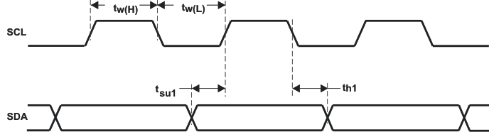 Figure 1. SCL and SDA Timing
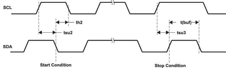 Figure 2. Start and Stop Conditions Timing
6.7 Typical Characteristics
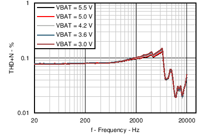
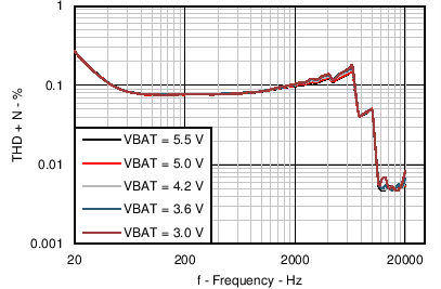
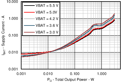
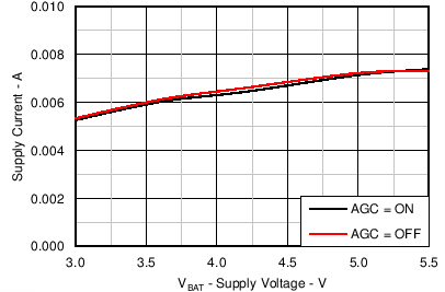
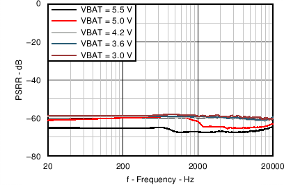
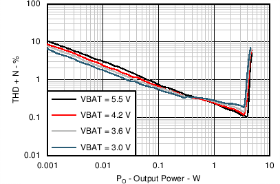
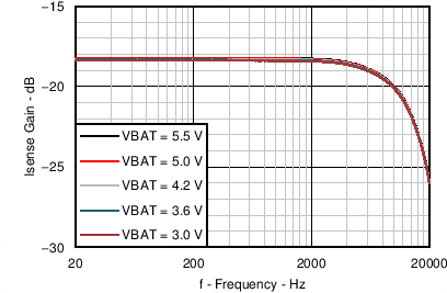
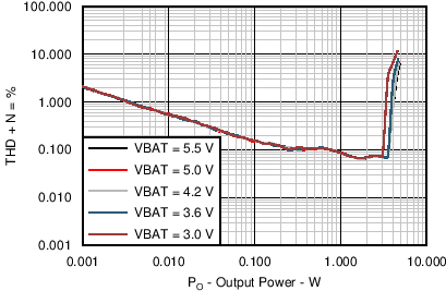
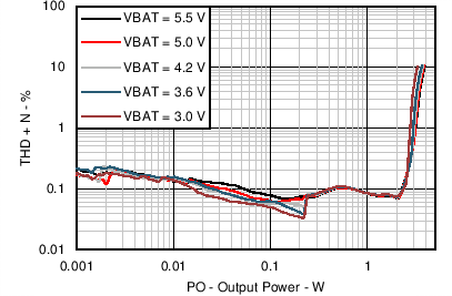
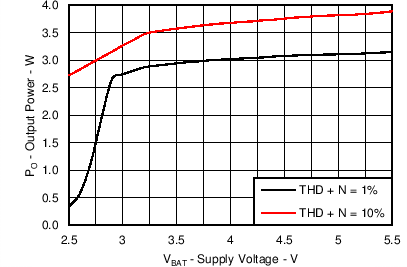
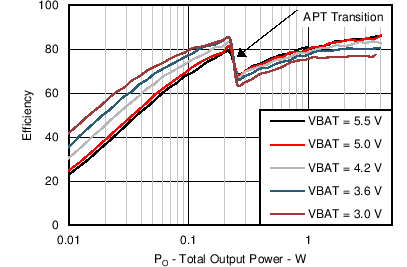
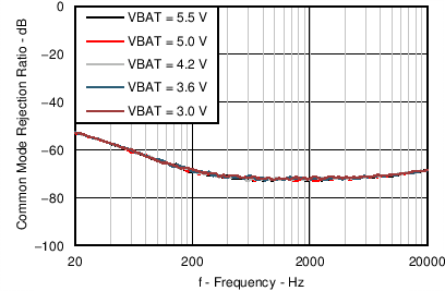
VBAT = 3.6 V, AVDD = IOVDD = 1.8 V, EN = IOVDD, SWS = 0, RL = 8 Ω + 33 µH (unless otherwise noted).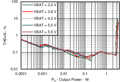
| AGC = OFF, Gain = 15 dB | ||
| AGC = OFF, Gain = 15 dB, Pout = 1 W | ||
| AGC = OFF, Gain = 15 dB | ||
| AGC = OFF, Gain = 15 dB, f = 1 kHz | ||
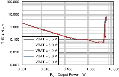
| VBAT = 3.0, 3.6, 4.2, 5.0, 5.5 V | ||
| 20 Hz to 20 kHz, Digital Input, Gain = 15 dB | ||
| AGC = OFF, Gain = 15 dB | ||
| 8 Ω Load, AGC = OFF, Gain = 15 dB | ||
| AGC = OFF, Input Level = -20 dBFS, Gain = 15 dB | ||
| f = 1 kHz, 0 dBFS Gain = 15 dB, | ||
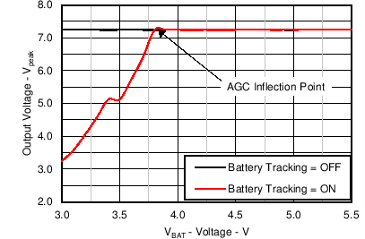
| Inflection point = 3.6 V, Slope = 4.5 V/V, No Load |

| AGC = OFF, Gain = 15 dB | ||
| AGC = OFF, Gain = 15 dB, f = 1 kHz | ||
| AGC = OFF, Gain = 15 dB, f = 1 kHz | ||
| AGC = OFF, Gain = 15 dB, f = 1 kHz | ||
| 20 Hz to 20 kHz, Analog Input, Gain = 15 dB | ||
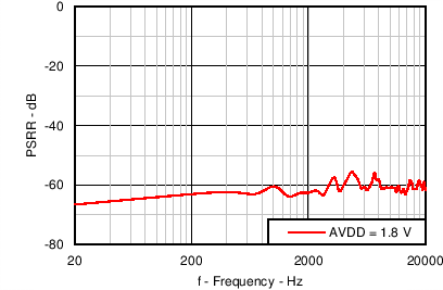
| 20 Hz to 20 kHz, Digital Input, AVDD = 1.8 V | ||
| AGC = OFF, Gain = 15 dB | ||
| AGC = OFF, Input Level = -20 dBFS, Gain = 15 dB | ||
| 8 Ω Load, AGC = OFF, Input Level = -20 dBFS, Gain = 15 dB | ||
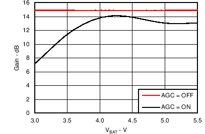
| AGC = ON, Gain = 15 dB, f = 1 kHz, Inflection point = 3.6 V | ||
| Limiter value = 7.87 V, Slope = 4.5 V |