SLASE86E June 2016 – December 2017 TAS2560
PRODUCTION DATA.
- 1 Features
- 2 Applications
- 3 Description
- 4 Revision History
- 5 Device Comparison Table
- 6 Pin Configuration and Functions
-
7 Specifications
- 7.1 Absolute Maximum Ratings
- 7.2 ESD Ratings
- 7.3 Recommended Operating Conditions
- 7.4 Thermal Information
- 7.5 Electrical Characteristics
- 7.6 I2C Timing Requirements
- 7.7 I2S/LJF/RJF Timing in Master Mode
- 7.8 I2S/LJF/RJF Timing in Slave Mode
- 7.9 DSP Timing in Master Mode
- 7.10 DSP Timing in Slave Mode
- 7.11 PDM Timing
- 7.12 Typical Characteristics
- 8 Parameter Measurement Information
-
9 Detailed Description
- 9.1 Overview
- 9.2 Functional Block Diagram
- 9.3
Feature Description
- 9.3.1 General I2C Operation
- 9.3.2 Single-Byte and Multiple-Byte Transfers
- 9.3.3 Single-Byte Write
- 9.3.4 Multiple-Byte Write and Incremental Multiple-Byte Write
- 9.3.5 Single-Byte Read
- 9.3.6 Multiple-Byte Read
- 9.3.7 PLL
- 9.3.8 Clock Distribution
- 9.3.9 Clock Error Detection
- 9.3.10 Class-D Edge Rate Control
- 9.3.11 IV Sense
- 9.3.12 Boost Control
- 9.3.13 Thermal Fold-back
- 9.3.14 Battery Guard AGC
- 9.3.15 Configurable Boost Current Limit (ILIM)
- 9.3.16 Fault Protection
- 9.3.17 Spread Spectrum vs Synchronized
- 9.3.18 IRQs and Flags
- 9.3.19 CRC checksum for I2C
- 9.3.20 PurePath Console 3 Software TAS2560 Application
- 9.4 Device Functional Modes
- 9.5 Operational Modes
- 9.6 Programming
- 9.7
Register Map
- 9.7.1 Register Map Summary
- 9.7.2 PAGE (book=0x00 page=0x00 address=0x00) [reset=0h]
- 9.7.3 RESET (book=0x00 page=0x00 address=0x01) [reset=0h]
- 9.7.4 MODE (book=0x00 page=0x00 address=0x02) [reset=1h]
- 9.7.5 SPK_CTRL (book=0x00 page=0x00 address=0x04) [reset=5Fh]
- 9.7.6 PWR_CTRL_2 (book=0x00 page=0x00 address=0x05) [reset=0h]
- 9.7.7 PWR_CTRL_1 (book=0x00 page=0x00 address=0x07) [reset=0h]
- 9.7.8 RAMP_CTRL (book=0x00 page=0x00 address=0x08) [reset=1h]
- 9.7.9 EDGE_ISNS_BOOST (book=0x00 page=0x00 address=0x09) [reset=83h]
- 9.7.10 PLL_CLKIN (book=0x00 page=0x00 address=0x0F) [reset=41h]
- 9.7.11 PLL_JVAL (book=0x00 page=0x00 address=0x10) [reset=4h]
- 9.7.12 PLL_DVAL_1 (book=0x00 page=0x00 address=0x11) [reset=0h]
- 9.7.13 PLL_DVAL_2 (book=0x00 page=0x00 address=0x12) [reset=0h]
- 9.7.14 ASI_FORMAT (book=0x00 page=0x00 address=0x14) [reset=2h]
- 9.7.15 ASI_CHANNEL (book=0x00 page=0x00 address=0x15) [reset=0h]
- 9.7.16 ASI_OFFSET_1 (book=0x00 page=0x00 address=0x16) [reset=0h]
- 9.7.17 ASI_OFFSET_2 (book=0x00 page=0x00 address=0x17) [reset=0h]
- 9.7.18 ASI_CFG_1 (book=0x00 page=0x00 address=0x18) [reset=0h]
- 9.7.19 ASI_DIV_SRC (book=0x00 page=0x00 address=0x19) [reset=0h]
- 9.7.20 ASI_BDIV (book=0x00 page=0x00 address=0x1A) [reset=1h]
- 9.7.21 ASI_WDIV (book=0x00 page=0x00 address=0x1B) [reset=40h]
- 9.7.22 PDM_CFG (book=0x00 page=0x00 address=0x1C) [reset=0h]
- 9.7.23 PDM_DIV (book=0x00 page=0x00 address=0x1D) [reset=8h]
- 9.7.24 DSD_DIV (book=0x00 page=0x00 address=0x1E) [reset=8h]
- 9.7.25 CLK_ERR_1 (book=0x00 page=0x00 address=0x21) [reset=3h]
- 9.7.26 CLK_ERR_2 (book=0x00 page=0x00 address=0x22) [reset=3Fh]
- 9.7.27 IRQ_PIN_CFG (book=0x00 page=0x00 address=0x23) [reset=21h]
- 9.7.28 INT_CFG_1 (book=0x00 page=0x00 address=0x24) [reset=0h]
- 9.7.29 INT_CFG_2 (book=0x00 page=0x00 address=0x25) [reset=0h]
- 9.7.30 INT_DET_1 (book=0x00 page=0x00 address=0x26) [reset=0h]
- 9.7.31 INT_DET_2 (book=0x00 page=0x00 address=0x27) [reset=0h]
- 9.7.32 STATUS_POWER (book=0x00 page=0x00 address=0x2A) [reset=0h]
- 9.7.33 SAR_VBAT_MSB (book=0x00 page=0x00 address=0x2D) [reset=C0h]
- 9.7.34 SAR_VBAT_LSB (book=0x00 page=0x00 address=0x2E) [reset=0h]
- 9.7.35 DIE_TEMP_SENSOR (book=0x00 page=0x00 address=0x31) [reset=0h]
- 9.7.36 LOW_PWR_MODE (book=0x00 page=0x00 address=0x35) [reset=0h]
- 9.7.37 PCM_RATE (book=0x00 page=0x00 address=0x36) [reset=32h]
- 9.7.38 CLOCK_ERR_CFG_1 (book=0x00 page=0x00 address=0x4F) [reset=0h]
- 9.7.39 CLOCK_ERR_CFG_2 (book=0x00 page=0x00 address=0x50) [reset=11h]
- 9.7.40 PROTECTION_CFG_1 (book=0x00 page=0x00 address=0x58) [reset=3h]
- 9.7.41 CRC_CHECKSUM (book=0x00 page=0x00 address=0x7E) [reset=0h]
- 9.7.42 BOOK (book=0x00 page=0x00 address=0x7F) [reset=0h]
- 10Application and Implementation
- 11Power Supply Recommendations
- 12Layout
- 13Device and Documentation Support
- 14Mechanical, Packaging, and Orderable Information
Package Options
Refer to the PDF data sheet for device specific package drawings
Mechanical Data (Package|Pins)
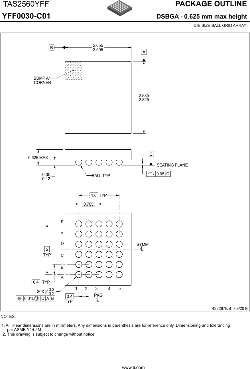
- YFF|30
Thermal pad, mechanical data (Package|Pins)
Orderable Information
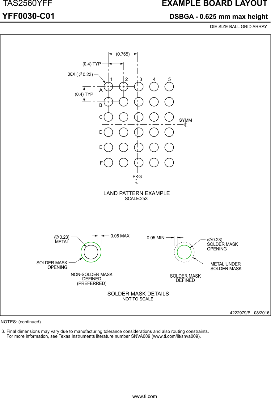
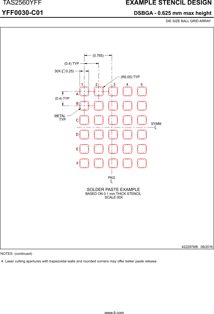
14 Mechanical, Packaging, and Orderable Information
The following pages include mechanical, packaging, and orderable information. This information is the most current data available for the designated devices. This data is subject to change without notice and revision of this document. For browser-based versions of this data sheet, refer to the left-hand navigation.


