SLASE86E June 2016 – December 2017 TAS2560
PRODUCTION DATA.
- 1 Features
- 2 Applications
- 3 Description
- 4 Revision History
- 5 Device Comparison Table
- 6 Pin Configuration and Functions
-
7 Specifications
- 7.1 Absolute Maximum Ratings
- 7.2 ESD Ratings
- 7.3 Recommended Operating Conditions
- 7.4 Thermal Information
- 7.5 Electrical Characteristics
- 7.6 I2C Timing Requirements
- 7.7 I2S/LJF/RJF Timing in Master Mode
- 7.8 I2S/LJF/RJF Timing in Slave Mode
- 7.9 DSP Timing in Master Mode
- 7.10 DSP Timing in Slave Mode
- 7.11 PDM Timing
- 7.12 Typical Characteristics
- 8 Parameter Measurement Information
-
9 Detailed Description
- 9.1 Overview
- 9.2 Functional Block Diagram
- 9.3
Feature Description
- 9.3.1 General I2C Operation
- 9.3.2 Single-Byte and Multiple-Byte Transfers
- 9.3.3 Single-Byte Write
- 9.3.4 Multiple-Byte Write and Incremental Multiple-Byte Write
- 9.3.5 Single-Byte Read
- 9.3.6 Multiple-Byte Read
- 9.3.7 PLL
- 9.3.8 Clock Distribution
- 9.3.9 Clock Error Detection
- 9.3.10 Class-D Edge Rate Control
- 9.3.11 IV Sense
- 9.3.12 Boost Control
- 9.3.13 Thermal Fold-back
- 9.3.14 Battery Guard AGC
- 9.3.15 Configurable Boost Current Limit (ILIM)
- 9.3.16 Fault Protection
- 9.3.17 Spread Spectrum vs Synchronized
- 9.3.18 IRQs and Flags
- 9.3.19 CRC checksum for I2C
- 9.3.20 PurePath Console 3 Software TAS2560 Application
- 9.4 Device Functional Modes
- 9.5 Operational Modes
- 9.6 Programming
- 9.7
Register Map
- 9.7.1 Register Map Summary
- 9.7.2 PAGE (book=0x00 page=0x00 address=0x00) [reset=0h]
- 9.7.3 RESET (book=0x00 page=0x00 address=0x01) [reset=0h]
- 9.7.4 MODE (book=0x00 page=0x00 address=0x02) [reset=1h]
- 9.7.5 SPK_CTRL (book=0x00 page=0x00 address=0x04) [reset=5Fh]
- 9.7.6 PWR_CTRL_2 (book=0x00 page=0x00 address=0x05) [reset=0h]
- 9.7.7 PWR_CTRL_1 (book=0x00 page=0x00 address=0x07) [reset=0h]
- 9.7.8 RAMP_CTRL (book=0x00 page=0x00 address=0x08) [reset=1h]
- 9.7.9 EDGE_ISNS_BOOST (book=0x00 page=0x00 address=0x09) [reset=83h]
- 9.7.10 PLL_CLKIN (book=0x00 page=0x00 address=0x0F) [reset=41h]
- 9.7.11 PLL_JVAL (book=0x00 page=0x00 address=0x10) [reset=4h]
- 9.7.12 PLL_DVAL_1 (book=0x00 page=0x00 address=0x11) [reset=0h]
- 9.7.13 PLL_DVAL_2 (book=0x00 page=0x00 address=0x12) [reset=0h]
- 9.7.14 ASI_FORMAT (book=0x00 page=0x00 address=0x14) [reset=2h]
- 9.7.15 ASI_CHANNEL (book=0x00 page=0x00 address=0x15) [reset=0h]
- 9.7.16 ASI_OFFSET_1 (book=0x00 page=0x00 address=0x16) [reset=0h]
- 9.7.17 ASI_OFFSET_2 (book=0x00 page=0x00 address=0x17) [reset=0h]
- 9.7.18 ASI_CFG_1 (book=0x00 page=0x00 address=0x18) [reset=0h]
- 9.7.19 ASI_DIV_SRC (book=0x00 page=0x00 address=0x19) [reset=0h]
- 9.7.20 ASI_BDIV (book=0x00 page=0x00 address=0x1A) [reset=1h]
- 9.7.21 ASI_WDIV (book=0x00 page=0x00 address=0x1B) [reset=40h]
- 9.7.22 PDM_CFG (book=0x00 page=0x00 address=0x1C) [reset=0h]
- 9.7.23 PDM_DIV (book=0x00 page=0x00 address=0x1D) [reset=8h]
- 9.7.24 DSD_DIV (book=0x00 page=0x00 address=0x1E) [reset=8h]
- 9.7.25 CLK_ERR_1 (book=0x00 page=0x00 address=0x21) [reset=3h]
- 9.7.26 CLK_ERR_2 (book=0x00 page=0x00 address=0x22) [reset=3Fh]
- 9.7.27 IRQ_PIN_CFG (book=0x00 page=0x00 address=0x23) [reset=21h]
- 9.7.28 INT_CFG_1 (book=0x00 page=0x00 address=0x24) [reset=0h]
- 9.7.29 INT_CFG_2 (book=0x00 page=0x00 address=0x25) [reset=0h]
- 9.7.30 INT_DET_1 (book=0x00 page=0x00 address=0x26) [reset=0h]
- 9.7.31 INT_DET_2 (book=0x00 page=0x00 address=0x27) [reset=0h]
- 9.7.32 STATUS_POWER (book=0x00 page=0x00 address=0x2A) [reset=0h]
- 9.7.33 SAR_VBAT_MSB (book=0x00 page=0x00 address=0x2D) [reset=C0h]
- 9.7.34 SAR_VBAT_LSB (book=0x00 page=0x00 address=0x2E) [reset=0h]
- 9.7.35 DIE_TEMP_SENSOR (book=0x00 page=0x00 address=0x31) [reset=0h]
- 9.7.36 LOW_PWR_MODE (book=0x00 page=0x00 address=0x35) [reset=0h]
- 9.7.37 PCM_RATE (book=0x00 page=0x00 address=0x36) [reset=32h]
- 9.7.38 CLOCK_ERR_CFG_1 (book=0x00 page=0x00 address=0x4F) [reset=0h]
- 9.7.39 CLOCK_ERR_CFG_2 (book=0x00 page=0x00 address=0x50) [reset=11h]
- 9.7.40 PROTECTION_CFG_1 (book=0x00 page=0x00 address=0x58) [reset=3h]
- 9.7.41 CRC_CHECKSUM (book=0x00 page=0x00 address=0x7E) [reset=0h]
- 9.7.42 BOOK (book=0x00 page=0x00 address=0x7F) [reset=0h]
- 10Application and Implementation
- 11Power Supply Recommendations
- 12Layout
- 13Device and Documentation Support
- 14Mechanical, Packaging, and Orderable Information
Package Options
Refer to the PDF data sheet for device specific package drawings
Mechanical Data (Package|Pins)
- YFF|30
Thermal pad, mechanical data (Package|Pins)
Orderable Information
11 Power Supply Recommendations
11.1 Power Supplies
The TAS2560 requires four power supplies:
- Boost Input (terminal: VBAT)
- Voltage: 2.9 V to 5.5 V
- Max Current: 5 A for ILIM = 3.0 A (default)
- Analog Supply (terminal: VDD)
- Voltage: 1.65 V to 1.95 V
- Max Current: 30 mA
- Digital I/O Supply (terminal: IOVDD)
- Voltage: 1.62 V to 3.6 V
- Max Current: 5 mA
The decoupling capacitors for the power supplies should be placed close to the device terminals. For VBAT, IOVDD, and VDD, a small decoupling capacitor of 0.1 µF should be placed as close as possible to the device terminals. Refer to Figure 100 for the schematic.
11.2 Power Supply Sequencing
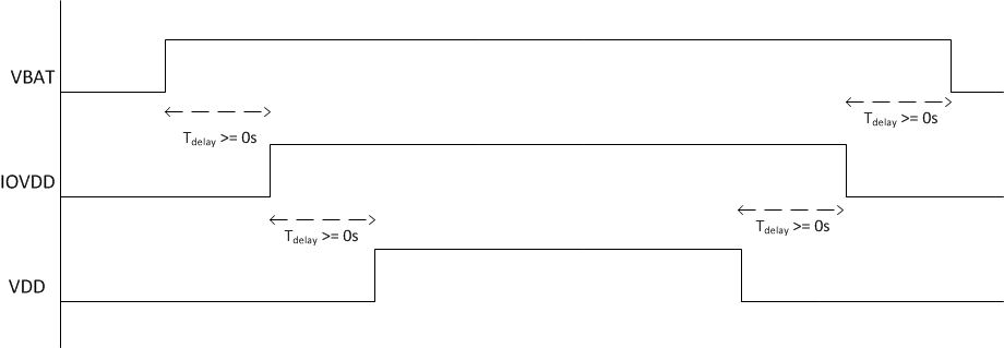
The following power sequence should be followed for power up and power down. If the recommended sequence is not followed there can be large current in device due to faults in level shifters and diodes becoming forward biased. The Tdelay between power supplies should be large enough for the power rails to settle.
 Figure 100. Power Supply Sequence for Power-Up and Power-Down
When the supplies have settled, the RESETZ terminal can be set HIGH to operate the device. Additionally the RESETZ pin can be tied to IOVDD and the internal DVDD POR will perform a reset of the device. After a hardware or software reset additional commands to the device should be delayed for 100uS to allow the OTP to load. The above sequence should be completed before any I2C operation.
11.2.1 Boost Supply Details
The boost supply (VBAT) and associated passives need to be able to support the current requirements of the device. By default, the peak current limit of the boost is set to 3 A. Refer to Configurable Boost Current Limit (ILIM) for information on changing the current limit. A minimum of a 10 µF capacitor is recommended on the boost supply to quickly support changes in required current. Refer to for the schematic.
The current requirements can also be reduced by lowering the gain of the amplifier, or in response to decreasing battery through the use of the battery-tracking AGC feature of the TAS2560 described in Battery Guard AGC.