SNAS854 February   2023 TDC1000-Q1

PRODUCTION DATA  

  1. Features
  2. Applications
  3. Description
  4. Revision History
  5. Pin Configuration and Functions
  6. Specifications
    1. 6.1 Absolute Maximum Ratings
    2. 6.2 ESD Ratings
    3. 6.3 Recommended Operating Conditions
    4. 6.4 Thermal Information (1)
    5. 6.5 Electrical Characteristics
    6. 6.6 Timing Requirements
    7. 6.7 Switching Characteristics
    8. 6.8 Typical Characteristics
  7. Parameter Measurement Information
  8. Detailed Description
    1. 8.1 Overview
    2. 8.2 Functional Block Diagram
    3. 8.3 Feature Description
      1. 8.3.1 Transmitter Signal Path
      2. 8.3.2 Receiver Signal Path
      3. 8.3.3 Low Noise Amplifier (LNA)
      4. 8.3.4 Programmable Gain Amplifier (PGA)
      5. 8.3.5 Receiver Filters
      6. 8.3.6 Comparators for STOP Pulse Generation
        1. 8.3.6.1 Threshold Detector and DAC
        2. 8.3.6.2 Zero-Cross Detect Comparator
        3. 8.3.6.3 Event Manager
      7. 8.3.7 Common-Mode Buffer (VCOM)
      8. 8.3.8 Temperature Sensor
        1. 8.3.8.1 Temperature Measurement With Multiple RTDs
        2. 8.3.8.2 Temperature Measurement With a Single RTD
    4. 8.4 Device Functional Modes
      1. 8.4.1 Time-of-Flight Measurement Mode
        1. 8.4.1.1 Mode 0
        2. 8.4.1.2 Mode 1
        3. 8.4.1.3 Mode 2
      2. 8.4.2 State Machine
      3. 8.4.3 TRANSMIT Operation
        1. 8.4.3.1 Transmission Pulse Count
        2. 8.4.3.2 TX 180° Pulse Shift
        3. 8.4.3.3 Transmitter Damping
      4. 8.4.4 RECEIVE Operation
        1. 8.4.4.1 Single Echo Receive Mode
        2. 8.4.4.2 Multiple Echo Receive Mode
      5. 8.4.5 Timing
        1. 8.4.5.1 Timing Control and Frequency Scaling (CLKIN)
        2. 8.4.5.2 TX/RX Measurement Sequencing and Timing
      6. 8.4.6 Time-of-Flight (TOF) Control
        1. 8.4.6.1 Short TOF Measurement
        2. 8.4.6.2 Standard TOF Measurement
        3. 8.4.6.3 Standard TOF Measurement With Power Blanking
        4. 8.4.6.4 Common-Mode Reference Settling Time
        5. 8.4.6.5 TOF Measurement Interval
      7. 8.4.7 Averaging and Channel Selection
      8. 8.4.8 Error Reporting
    5. 8.5 Programming
      1. 8.5.1 Serial Peripheral Interface (SPI)
        1. 8.5.1.1 Chip Select Bar (CSB)
        2. 8.5.1.2 Serial Clock (SCLK)
        3. 8.5.1.3 Serial Data Input (SDI)
        4. 8.5.1.4 Serial Data Output (SDO)
    6. 8.6 Register Maps
  9. Application and Implementation
    1. 9.1 Application Information
    2. 9.2 Typical Applications
      1. 9.2.1 Level and Fluid Identification Measurements
        1. 9.2.1.1 Design Requirements
        2. 9.2.1.2 Detailed Design Procedure
          1. 9.2.1.2.1 Level Measurements
          2. 9.2.1.2.2 Fluid Identification
        3. 9.2.1.3 Application Curves
      2. 9.2.2 Water Flow Metering
        1. 9.2.2.1 Design Requirements
        2. 9.2.2.2 Detailed Design Procedure
          1. 9.2.2.2.1 Regulations and Accuracy
          2. 9.2.2.2.2 Transit-Time in Ultrasonic Flow Meters
          3. 9.2.2.2.3 ΔTOF Accuracy Requirement Calculation
          4. 9.2.2.2.4 Operation
        3. 9.2.2.3 Application Curves
    3. 9.3 Power Supply Recommendations
    4. 9.4 Layout
      1. 9.4.1 Layout Guidelines
      2. 9.4.2 Layout Example
  10. 10Device and Documentation Support
    1. 10.1 Device Support
      1. 10.1.1 Development Support
    2. 10.2 Receiving Notification of Documentation Updates
    3. 10.3 Support Resources
    4. 10.4 Trademarks
    5. 10.5 Electrostatic Discharge Caution
    6. 10.6 Glossary
  11. 11Mechanical, Packaging, and Orderable Information

Package Options

Mechanical Data (Package|Pins)
Thermal pad, mechanical data (Package|Pins)
Orderable Information

Typical Characteristics

At TA = 25°C, unless otherwise noted.
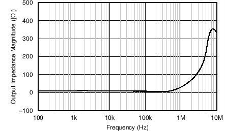
GUID-F14E396A-8C53-4A14-9616-0432659B194E-low.png
VDD = VIO = 3.7 VCapacitive Feedback ModeRL = 1 kΩ
Figure 6-2 LNA ZOUT vs Frequency
GUID-9D9AD30E-5B3D-473A-B13F-34AADF67A3E6-low.png
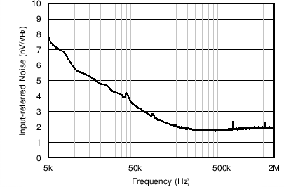
VDD = VIO = 3.1 VCapacitive Feedback ModeRL = ∞
Figure 6-4 LNA Input-Referred Noise vs Frequency
GUID-C5BA0E22-177E-40D1-80EB-452A2C8CDE19-low.png
VDD = VIO = 3.7 VResistive Feedback ModeRL = 1 kΩ
VIN = 100 mVfIN = 100 kHz
Figure 6-6 LNA Response
GUID-46D490DD-F1A1-4532-8BCE-18D2D01A5058-low.png
VDD = VIO = 3.7 VCapacitive Feedback ModeRL = 100 kΩ
CIN = 300 pF
Figure 6-8 LNA Gain vs Frequency
GUID-5BBE8F21-DD6A-480E-8A11-EB5518980ECE-low.png
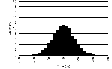
VDD = VIO = 5 VLNA Capacitive Feedback ModePGA Gain of 6 dB
VIN = 100 mVfIN = 1 MHz
(See GUID-72D520D8-3AB2-4ABC-B20F-282E41D31FC0.html#SNAS6485768)Count ≥ 10000
Figure 6-10 RX Jitter Histogram
GUID-E4BBF424-A7FD-4113-9842-4D71559BD3FE-low.png
VDD = VIO = 3.7 VLNA Capacitive Feedback ModePGA Gain of 6 dB
VIN = 100 mVfIN = 1 MHz
TA = –40°C(See GUID-72D520D8-3AB2-4ABC-B20F-282E41D31FC0.html#SNAS6485768)Count ≥ 10000
Figure 6-12 RX Jitter Histogram
GUID-65EDB239-CD93-4B10-80C7-AC3CBD5621AF-low.png
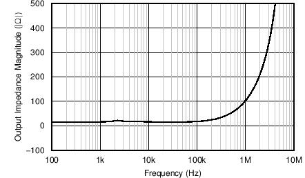
VDD = VIO = 3.7 VGain of 21 dBRL = 1 kΩ
Figure 6-3 PGA ZOUT vs Frequency
GUID-F479B0CC-3447-4807-9F9C-1101587247A1-low.png
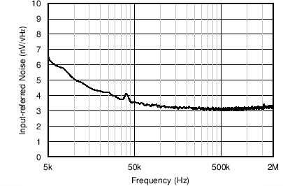
VDD = VIO = 3.7 VGain of 21 dBRL = ∞
Figure 6-5 PGA Input-Referred Noise vs Frequency
GUID-07E66797-A986-48EB-B289-0AC7FE63F133-low.png
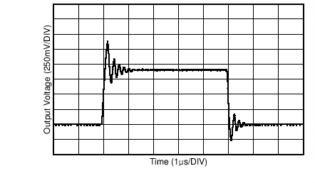
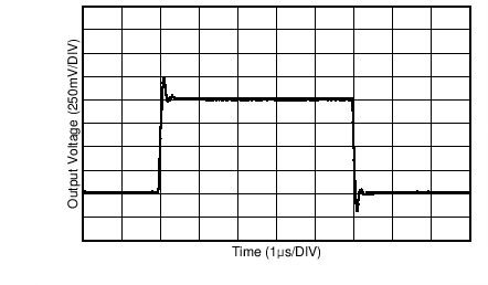
VDD = VIO = 3.7 VGain of 21 dBRL = 100 kΩ
VIN = 100 mVfIN = 100 kHz
Figure 6-7 PGA Response
GUID-34ED8ECD-297C-44BA-A3A1-B4A992441CA5-low.png
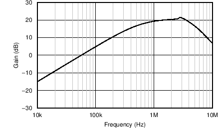
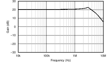
VDD = VIO = 3.7 VGain of 21 dBRL = 100 kΩ
Figure 6-9 PGA Gain vs Frequency
GUID-2E7AD3CA-0F0A-4100-8B05-94D2AA3063B9-low.png
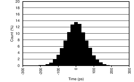
VDD = VIO = 3.7 VLNA Capacitive Feedback ModePGA Gain of 6 dB
VIN = 100 mVfIN = 1 MHz
TA = 25°C(See GUID-72D520D8-3AB2-4ABC-B20F-282E41D31FC0.html#SNAS6485768)Count ≥ 10000
Figure 6-11 RX Jitter Histogram
GUID-B97F22A3-475C-4F0C-834E-21EE6E90F14B-low.png
VDD = VIO = 3.7 VLNA Capacitive Feedback ModePGA Gain of 6 dB
VIN = 100 mVfIN = 1 MHz
TA = 125°C(See GUID-72D520D8-3AB2-4ABC-B20F-282E41D31FC0.html#SNAS6485768)Count ≥ 10000
Figure 6-13 RX Jitter Histogram