SNAS854 February   2023 TDC1000-Q1

PRODUCTION DATA  

  1. Features
  2. Applications
  3. Description
  4. Revision History
  5. Pin Configuration and Functions
  6. Specifications
    1. 6.1 Absolute Maximum Ratings
    2. 6.2 ESD Ratings
    3. 6.3 Recommended Operating Conditions
    4. 6.4 Thermal Information (1)
    5. 6.5 Electrical Characteristics
    6. 6.6 Timing Requirements
    7. 6.7 Switching Characteristics
    8. 6.8 Typical Characteristics
  7. Parameter Measurement Information
  8. Detailed Description
    1. 8.1 Overview
    2. 8.2 Functional Block Diagram
    3. 8.3 Feature Description
      1. 8.3.1 Transmitter Signal Path
      2. 8.3.2 Receiver Signal Path
      3. 8.3.3 Low Noise Amplifier (LNA)
      4. 8.3.4 Programmable Gain Amplifier (PGA)
      5. 8.3.5 Receiver Filters
      6. 8.3.6 Comparators for STOP Pulse Generation
        1. 8.3.6.1 Threshold Detector and DAC
        2. 8.3.6.2 Zero-Cross Detect Comparator
        3. 8.3.6.3 Event Manager
      7. 8.3.7 Common-Mode Buffer (VCOM)
      8. 8.3.8 Temperature Sensor
        1. 8.3.8.1 Temperature Measurement With Multiple RTDs
        2. 8.3.8.2 Temperature Measurement With a Single RTD
    4. 8.4 Device Functional Modes
      1. 8.4.1 Time-of-Flight Measurement Mode
        1. 8.4.1.1 Mode 0
        2. 8.4.1.2 Mode 1
        3. 8.4.1.3 Mode 2
      2. 8.4.2 State Machine
      3. 8.4.3 TRANSMIT Operation
        1. 8.4.3.1 Transmission Pulse Count
        2. 8.4.3.2 TX 180° Pulse Shift
        3. 8.4.3.3 Transmitter Damping
      4. 8.4.4 RECEIVE Operation
        1. 8.4.4.1 Single Echo Receive Mode
        2. 8.4.4.2 Multiple Echo Receive Mode
      5. 8.4.5 Timing
        1. 8.4.5.1 Timing Control and Frequency Scaling (CLKIN)
        2. 8.4.5.2 TX/RX Measurement Sequencing and Timing
      6. 8.4.6 Time-of-Flight (TOF) Control
        1. 8.4.6.1 Short TOF Measurement
        2. 8.4.6.2 Standard TOF Measurement
        3. 8.4.6.3 Standard TOF Measurement With Power Blanking
        4. 8.4.6.4 Common-Mode Reference Settling Time
        5. 8.4.6.5 TOF Measurement Interval
      7. 8.4.7 Averaging and Channel Selection
      8. 8.4.8 Error Reporting
    5. 8.5 Programming
      1. 8.5.1 Serial Peripheral Interface (SPI)
        1. 8.5.1.1 Chip Select Bar (CSB)
        2. 8.5.1.2 Serial Clock (SCLK)
        3. 8.5.1.3 Serial Data Input (SDI)
        4. 8.5.1.4 Serial Data Output (SDO)
    6. 8.6 Register Maps
  9. Application and Implementation
    1. 9.1 Application Information
    2. 9.2 Typical Applications
      1. 9.2.1 Level and Fluid Identification Measurements
        1. 9.2.1.1 Design Requirements
        2. 9.2.1.2 Detailed Design Procedure
          1. 9.2.1.2.1 Level Measurements
          2. 9.2.1.2.2 Fluid Identification
        3. 9.2.1.3 Application Curves
      2. 9.2.2 Water Flow Metering
        1. 9.2.2.1 Design Requirements
        2. 9.2.2.2 Detailed Design Procedure
          1. 9.2.2.2.1 Regulations and Accuracy
          2. 9.2.2.2.2 Transit-Time in Ultrasonic Flow Meters
          3. 9.2.2.2.3 ΔTOF Accuracy Requirement Calculation
          4. 9.2.2.2.4 Operation
        3. 9.2.2.3 Application Curves
    3. 9.3 Power Supply Recommendations
    4. 9.4 Layout
      1. 9.4.1 Layout Guidelines
      2. 9.4.2 Layout Example
  10. 10Device and Documentation Support
    1. 10.1 Device Support
      1. 10.1.1 Development Support
    2. 10.2 Receiving Notification of Documentation Updates
    3. 10.3 Support Resources
    4. 10.4 Trademarks
    5. 10.5 Electrostatic Discharge Caution
    6. 10.6 Glossary
  11. 11Mechanical, Packaging, and Orderable Information

Package Options

Mechanical Data (Package|Pins)
Thermal pad, mechanical data (Package|Pins)
Orderable Information

Receiver Filters

TI recommends to place two filters in the RX path to minimize the receive path noise and obtain maximum timing accuracy. As shown in #SNAS6481456, one filter is placed between the LNAOUT and the PGAIN pins, and another filter is placed between the PGAOUT and the COMPIN pins.

With an in-band gain of 10, the LNA has a bandwidth of 5 MHz. For most applications, a low-pass filter between the LNAOUT and PGAIN pins is sufficient.

As shown in #SNAS6481456, the second filter stage can use a cascade of a low-pass filter (RF1 and CF3) followed by a high-pass filter (CF2 and RF2) referenced to VCOM. Design of the filter is straightforward. The RF1 and CF2 can be chosen first. A reasonable set of values for RF1 and CF2 could be: RF1 = 1 kΩ ± 10% and CF2 = 50pF ± 10%. Given the center frequency of interest to be ƒC and the filter bandwidth to be ƒB, the value of CF3 can be calculated as:

Equation 2. GUID-CCBE5E47-9D62-4A7A-8165-F38434E32366-low.gif

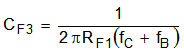
RF2 and CF2 determine the high-pass corner of the filter. RF2 should be referenced to VCOM to maintain the DC bias level at the comparator input during the echo receive time. For values of RF2 larger than RF1, there will be limited loading effect from the high-pass filter to the low-pass filter resulting in more accurate corner frequencies. The chosen values shown in the figure below result in a high-pass corner frequency of about 600 kHz and a low-pass corner frequency of about 3 MHz.

More complex filters can be used; external gain is acceptable if the signal amplitude is too low. If the pass-band of the filter is wider than an octave, TI recommends to use a filter design which has linear group delay.

GUID-A14B04CF-E4AC-4613-90C7-9DF886973D78-low.gifFigure 8-5 Filter for a 1-MHz Operation