SNAS854 February   2023 TDC1000-Q1

PRODUCTION DATA  

  1. Features
  2. Applications
  3. Description
  4. Revision History
  5. Pin Configuration and Functions
  6. Specifications
    1. 6.1 Absolute Maximum Ratings
    2. 6.2 ESD Ratings
    3. 6.3 Recommended Operating Conditions
    4. 6.4 Thermal Information (1)
    5. 6.5 Electrical Characteristics
    6. 6.6 Timing Requirements
    7. 6.7 Switching Characteristics
    8. 6.8 Typical Characteristics
  7. Parameter Measurement Information
  8. Detailed Description
    1. 8.1 Overview
    2. 8.2 Functional Block Diagram
    3. 8.3 Feature Description
      1. 8.3.1 Transmitter Signal Path
      2. 8.3.2 Receiver Signal Path
      3. 8.3.3 Low Noise Amplifier (LNA)
      4. 8.3.4 Programmable Gain Amplifier (PGA)
      5. 8.3.5 Receiver Filters
      6. 8.3.6 Comparators for STOP Pulse Generation
        1. 8.3.6.1 Threshold Detector and DAC
        2. 8.3.6.2 Zero-Cross Detect Comparator
        3. 8.3.6.3 Event Manager
      7. 8.3.7 Common-Mode Buffer (VCOM)
      8. 8.3.8 Temperature Sensor
        1. 8.3.8.1 Temperature Measurement With Multiple RTDs
        2. 8.3.8.2 Temperature Measurement With a Single RTD
    4. 8.4 Device Functional Modes
      1. 8.4.1 Time-of-Flight Measurement Mode
        1. 8.4.1.1 Mode 0
        2. 8.4.1.2 Mode 1
        3. 8.4.1.3 Mode 2
      2. 8.4.2 State Machine
      3. 8.4.3 TRANSMIT Operation
        1. 8.4.3.1 Transmission Pulse Count
        2. 8.4.3.2 TX 180° Pulse Shift
        3. 8.4.3.3 Transmitter Damping
      4. 8.4.4 RECEIVE Operation
        1. 8.4.4.1 Single Echo Receive Mode
        2. 8.4.4.2 Multiple Echo Receive Mode
      5. 8.4.5 Timing
        1. 8.4.5.1 Timing Control and Frequency Scaling (CLKIN)
        2. 8.4.5.2 TX/RX Measurement Sequencing and Timing
      6. 8.4.6 Time-of-Flight (TOF) Control
        1. 8.4.6.1 Short TOF Measurement
        2. 8.4.6.2 Standard TOF Measurement
        3. 8.4.6.3 Standard TOF Measurement With Power Blanking
        4. 8.4.6.4 Common-Mode Reference Settling Time
        5. 8.4.6.5 TOF Measurement Interval
      7. 8.4.7 Averaging and Channel Selection
      8. 8.4.8 Error Reporting
    5. 8.5 Programming
      1. 8.5.1 Serial Peripheral Interface (SPI)
        1. 8.5.1.1 Chip Select Bar (CSB)
        2. 8.5.1.2 Serial Clock (SCLK)
        3. 8.5.1.3 Serial Data Input (SDI)
        4. 8.5.1.4 Serial Data Output (SDO)
    6. 8.6 Register Maps
  9. Application and Implementation
    1. 9.1 Application Information
    2. 9.2 Typical Applications
      1. 9.2.1 Level and Fluid Identification Measurements
        1. 9.2.1.1 Design Requirements
        2. 9.2.1.2 Detailed Design Procedure
          1. 9.2.1.2.1 Level Measurements
          2. 9.2.1.2.2 Fluid Identification
        3. 9.2.1.3 Application Curves
      2. 9.2.2 Water Flow Metering
        1. 9.2.2.1 Design Requirements
        2. 9.2.2.2 Detailed Design Procedure
          1. 9.2.2.2.1 Regulations and Accuracy
          2. 9.2.2.2.2 Transit-Time in Ultrasonic Flow Meters
          3. 9.2.2.2.3 ΔTOF Accuracy Requirement Calculation
          4. 9.2.2.2.4 Operation
        3. 9.2.2.3 Application Curves
    3. 9.3 Power Supply Recommendations
    4. 9.4 Layout
      1. 9.4.1 Layout Guidelines
      2. 9.4.2 Layout Example
  10. 10Device and Documentation Support
    1. 10.1 Device Support
      1. 10.1.1 Development Support
    2. 10.2 Receiving Notification of Documentation Updates
    3. 10.3 Support Resources
    4. 10.4 Trademarks
    5. 10.5 Electrostatic Discharge Caution
    6. 10.6 Glossary
  11. 11Mechanical, Packaging, and Orderable Information

Package Options

Mechanical Data (Package|Pins)
Thermal pad, mechanical data (Package|Pins)
Orderable Information

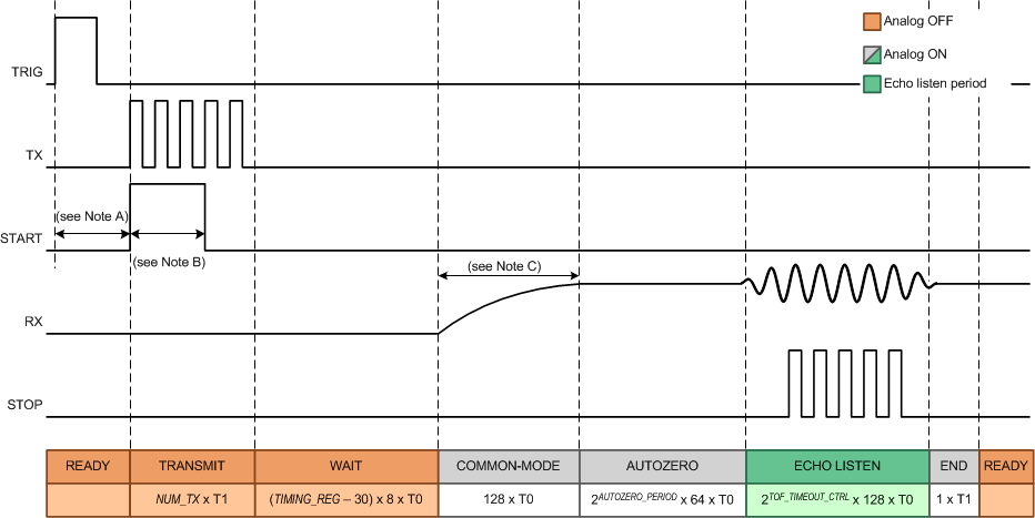
Standard TOF Measurement With Power Blanking

GUID-8B4254D1-77DF-4824-85D3-D796FD318D55-low.gif
If NUM_TX < 3, the width of the START pulse is equal to NUM_TX × T1. If NUM_TX ≥ 3, the width of the START pulse is equal to 3 × T1.
Common-mode settling time.
Figure 8-25 Standard TOF Measurement With Blanking Enabled

The power blanking sequence is a variation to the standard TOF measurement sequence, and can be enabled by setting the BLANKING bit to 1. In addition, all other conditions described in the GUID-A84C2F23-9217-4ED0-A094-C45409125914.html#TITLE-SNAS648SNAS6484638 should be met. The BLANKING bit can be found in the CONFIG_3 register.

Power blanking allows the device to remain in a low-power state while the TX signals propagate to the RX transducer in situations when the expected time-of-flight is long. Power blanking uses the TIMING_REG to control a wait time between the transmit sequence and the receive sequence, during which the complete RX chain is disabled (see #SNAS6488640). The TIMING_REG is a 10-bit wide field, with the two most significant bits located in the TOF_1 register, and the seven least significant bits located in the TOF_0 register.