SNAS648C October   2014  – February 2023 TDC1000

PRODUCTION DATA  

  1. Features
  2. Applications
  3. Description
  4. Revision History
  5. Pin Configuration and Functions
  6. Specifications
    1. 6.1 Absolute Maximum Ratings
    2. 6.2 ESD Ratings
    3. 6.3 Recommended Operating Conditions
    4. 6.4 Thermal Information (1)
    5. 6.5 Electrical Characteristics
    6. 6.6 Timing Requirements
    7. 6.7 Switching Characteristics
    8. 6.8 Typical Characteristics
  7. Parameter Measurement Information
  8. Detailed Description
    1. 8.1 Overview
    2. 8.2 Functional Block Diagram
    3. 8.3 Feature Description
      1. 8.3.1 Transmitter Signal Path
      2. 8.3.2 Receiver Signal Path
      3. 8.3.3 Low Noise Amplifier (LNA)
      4. 8.3.4 Programmable Gain Amplifier (PGA)
      5. 8.3.5 Receiver Filters
      6. 8.3.6 Comparators for STOP Pulse Generation
        1. 8.3.6.1 Threshold Detector and DAC
        2. 8.3.6.2 Zero-Cross Detect Comparator
        3. 8.3.6.3 Event Manager
      7. 8.3.7 Common-Mode Buffer (VCOM)
      8. 8.3.8 Temperature Sensor
        1. 8.3.8.1 Temperature Measurement With Multiple RTDs
        2. 8.3.8.2 Temperature Measurement With a Single RTD
    4. 8.4 Device Functional Modes
      1. 8.4.1 Time-of-Flight Measurement Mode
        1. 8.4.1.1 Mode 0
        2. 8.4.1.2 Mode 1
        3. 8.4.1.3 Mode 2
      2. 8.4.2 State Machine
      3. 8.4.3 TRANSMIT Operation
        1. 8.4.3.1 Transmission Pulse Count
        2. 8.4.3.2 TX 180° Pulse Shift
        3. 8.4.3.3 Transmitter Damping
      4. 8.4.4 RECEIVE Operation
        1. 8.4.4.1 Single Echo Receive Mode
        2. 8.4.4.2 Multiple Echo Receive Mode
      5. 8.4.5 Timing
        1. 8.4.5.1 Timing Control and Frequency Scaling (CLKIN)
        2. 8.4.5.2 TX/RX Measurement Sequencing and Timing
      6. 8.4.6 Time-of-Flight (TOF) Control
        1. 8.4.6.1 Short TOF Measurement
        2. 8.4.6.2 Standard TOF Measurement
        3. 8.4.6.3 Standard TOF Measurement With Power Blanking
        4. 8.4.6.4 Common-Mode Reference Settling Time
        5. 8.4.6.5 TOF Measurement Interval
      7. 8.4.7 Averaging and Channel Selection
      8. 8.4.8 Error Reporting
    5. 8.5 Programming
      1. 8.5.1 Serial Peripheral Interface (SPI)
        1. 8.5.1.1 Chip Select Bar (CSB)
        2. 8.5.1.2 Serial Clock (SCLK)
        3. 8.5.1.3 Serial Data Input (SDI)
        4. 8.5.1.4 Serial Data Output (SDO)
    6. 8.6 Register Maps
  9. Application and Implementation
    1. 9.1 Application Information
    2. 9.2 Typical Applications
      1. 9.2.1 Level and Fluid Identification Measurements
        1. 9.2.1.1 Design Requirements
        2. 9.2.1.2 Detailed Design Procedure
          1. 9.2.1.2.1 Level Measurements
          2. 9.2.1.2.2 Fluid Identification
        3. 9.2.1.3 Application Curves
      2. 9.2.2 Water Flow Metering
        1. 9.2.2.1 Design Requirements
        2. 9.2.2.2 Detailed Design Procedure
          1. 9.2.2.2.1 Regulations and Accuracy
          2. 9.2.2.2.2 Transit-Time in Ultrasonic Flow Meters
          3. 9.2.2.2.3 ΔTOF Accuracy Requirement Calculation
          4. 9.2.2.2.4 Operation
        3. 9.2.2.3 Application Curves
    3. 9.3 Power Supply Recommendations
    4. 9.4 Layout
      1. 9.4.1 Layout Guidelines
      2. 9.4.2 Layout Example
  10. 10Device and Documentation Support
    1. 10.1 Device Support
      1. 10.1.1 Development Support
    2. 10.2 Receiving Notification of Documentation Updates
    3. 10.3 Support Resources
    4. 10.4 Trademarks
    5. 10.5 Electrostatic Discharge Caution
    6. 10.6 Glossary
  11. 11Mechanical, Packaging, and Orderable Information

Package Options

Mechanical Data (Package|Pins)
Thermal pad, mechanical data (Package|Pins)
Orderable Information

Low Noise Amplifier (LNA)

The LNA in the TDC1000 front-end limits the input-referred noise and ensures timing accuracy for the generated STOP pulses. The LNA is an inverting amplifier designed for a closed-loop gain of 20 dB with the aid of an external input capacitor or resistor, and the LNA can be programmed for two feedback configurations. The band-pass configuration, referred to as capacitive feedback mode, must be combined with an input capacitor. The low-pass configuration, referred to as resistive feedback mode, must be combined with an input resistor. The recommended values for the input components are 300 pF and 900 Ω, respectively.

The LNA can be configured in capacitive feedback mode for transducers with resonant frequencies in the order of a couple of MHz. This is done by clearing the LNA_FB bit in the TOF_1 register to 0. As shown in #SNAS6482760, the external capacitor, CIN, should be placed between the transducer and the corresponding input pin. This provides an in-band gain of CIN/CF, where CF is the on-chip 30-pF feedback capacitor. Provided that CIN = 300 pF, the in-band gain of the LNA circuit is:

Equation 1. GUID-E67FC10A-F983-4167-9E3A-EF37D6D04F00-low.gif
GUID-8605284F-6BDA-4560-865D-4D4A20C430C1-low.gif 
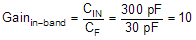
Figure 8-2 LNA Capacitive Feedback Configuration

The capacitive feedback configuration of the LNA has a band-pass frequency response. The high-pass corner frequency is set by the internal feedback components RF (9 kΩ) and CF (30 pF), and is approximately 590 kHz. The in-band gain is set by the capacitor ratio and the LNA’s 50-MHz gain-bandwidth product sets the low-pass corner of the frequency response. For example, an in-band gain of 10 results in a bandpass response between 590 kHz and 5 MHz.

The LNA can be configured in resistive feedback mode for transducers with resonant frequencies in the order of a couple of hundreds of kHz. This is done by setting the LNA_FB bit in the TOF_1 register to 1. In this configuration, the internal feedback capacitor CF is disconnected (see #SNAS6483714), and the DC gain of the LNA circuit is determined by the ratio between the internal feedback resistor RF (9 kΩ) and an external resistor RIN. For RIN = 900 Ω, the gain of the circuit is 10.

GUID-5509BD5E-B05C-48FC-A82E-189CF9EA7296-low.gif Figure 8-3 LNA Resistive Feedback Configuration

The LNA can be bypassed and disabled by writing a 1 to the LNA_CTRL bit in the TOF_1 register.