SLOSE89A November   2021  – March 2022 THS4541-DIE

PRODUCTION DATA  

  1. Features
  2. Applications
  3. Description
  4. Revision History
  5. Bare Die Information
  6. Pin Configuration and Functions
  7. Specifications
    1. 7.1 Absolute Maximum Ratings
    2. 7.2 Recommended Operating Conditions
    3. 7.3 Electrical Characteristics: (Vs+) - Vs- = 5 V
    4. 7.4 Typical Characteristics 5-V Single Supply
    5. 7.5 Typical Characteristics: 3-V to 5-V Supply Range
  8. Detailed Description
    1. 8.1 Overview
      1. 8.1.1 Terminology and Application Assumptions
    2. 8.2 Functional Block Diagram
    3. 8.3 Feature Description
      1. 8.3.1 Differential I/O
      2. 8.3.2 Power-Down Control Pin (PD)
        1. 8.3.2.1 Operating the Power Shutdown Feature
      3. 8.3.3 Input Overdrive Operation
    4. 8.4 Device Functional Modes
      1. 8.4.1 Operation from Single-Ended Sources to Differential Outputs
  9. Application and Implementation
    1. 9.1 Application Information
    2. 9.2 Typical Applications
      1. 9.2.1 Interfacing to High-Performance ADCs
        1. 9.2.1.1 Design Requirements
        2. 9.2.1.2 Detailed Design Procedure
        3. 9.2.1.3 Application Curve
  10. 10Power Supply Recommendations
  11. 11Layout
    1. 11.1 Layout Guidelines
  12. 12Device and Documentation Support
    1. 12.1 Device Support
      1. 12.1.1 Development Support
        1. 12.1.1.1 TINA Simulation Model Features
    2. 12.2 Documentation Support
      1. 12.2.1 Related Documentation
    3. 12.3 Receiving Notification of Documentation Updates
    4. 12.4 Support Resources
    5. 12.5 Trademarks
    6. 12.6 Electrostatic Discharge Caution
    7. 12.7 Glossary
  13. 13Mechanical, Packaging, and Orderable Information

Package Options

Mechanical Data (Package|Pins)
  • Y|0
Thermal pad, mechanical data (Package|Pins)
Orderable Information

Typical Characteristics 5-V Single Supply

at Vs+ = 5 V, Vs– = GND, Vocm is open, 50-Ω single-ended input to differential output, RF = 402 Ω, Gain = 2 V/V, Rload = 500 Ω, and TA ≈ 25°C (unless otherwise noted)
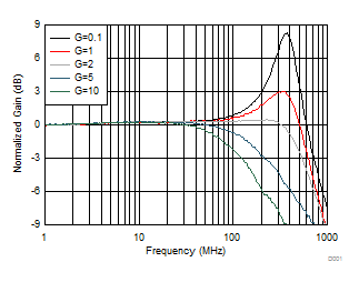
GUID-18F5EF82-2EF0-49E9-8F17-F83B591D6BB0-low.gif
Figure 7-1 Small-Signal Frequency Response vs Gain
GUID-15C15D0D-1747-436B-858A-1B12F9807A71-low.gif
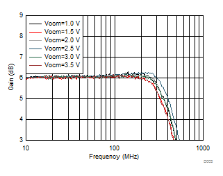
Vout = 100 mVPP
Figure 7-3 Small-Signal Frequency Response vs Vocm
GUID-A1C3D2F0-4A48-4F97-B850-CEEA9B2B431A-low.gif
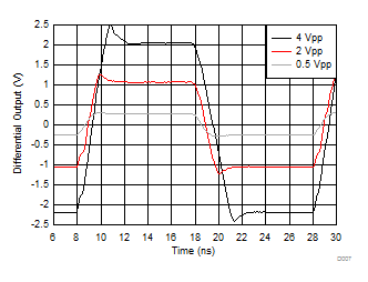
50-MHz input, 0.3-ns input edge rate, single-ended to differential output, DC coupled
Figure 7-5 Small- and Large-Signal Step Response
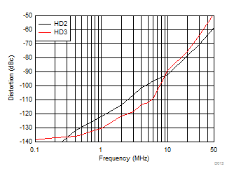
GUID-22607121-2C17-42C3-A4D2-D7FA38DB3068-low.gif
Vo = 2-VPP
Figure 7-7 Harmonic Distortion Over Frequency
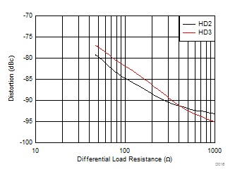
GUID-708F3812-74F3-4EC3-8707-B196E8472753-low.gif
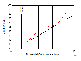
f = 10 MHz
Figure 7-9 Harmonic Distortion vs Rload
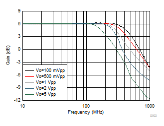
GUID-7E5A866D-0FBA-41BD-B584-DC878679ABE9-low.gif
Figure 7-2 Frequency Response vs Vopp
GUID-B5F0A5BF-B5C9-439F-9A67-B01CA2C00503-low.gif
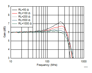
Vout = 100 mVPP
Figure 7-4 Small-Signal Frequency Response vs Rload (RL)
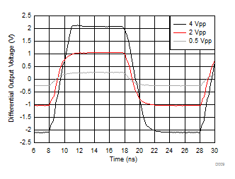
GUID-FA52F37A-7A1A-41CD-9473-D4E5A231361E-low.gif
G = 5 V/V, 50-MHz input, 0.3-ns input edge rate, single-ended input to differential output
Figure 7-6 Small- and Large-Signal Step Response
GUID-4D188397-D54F-48D8-8B84-CC28C7205021-low.gif
f = 10 MHz
Figure 7-8 Harmonic Distortion vs Output Swing
GUID-86C45BDE-9164-461D-9C29-9F786026D43F-low.gif
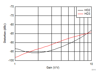
f = 10 MHz, Vo = 2-VPP
Figure 7-10 Harmonic Distortion vs Gain