SLOSE89A November 2021 – March 2022 THS4541-DIE
PRODUCTION DATA
- 1 Features
- 2 Applications
- 3 Description
- 4 Revision History
- 5 Bare Die Information
- 6 Pin Configuration and Functions
- 7 Specifications
- 8 Detailed Description
- 9 Application and Implementation
- 10Power Supply Recommendations
- 11Layout
- 12Device and Documentation Support
- 13Mechanical, Packaging, and Orderable Information
Package Options
Mechanical Data (Package|Pins)
- Y|0
Thermal pad, mechanical data (Package|Pins)
Orderable Information
3 Description
The THS4541-DIE is a low-power, voltage-feedback, fully differential amplifier (FDA) with an input common-mode range below the negative rail, and rail-to-rail output. This is a bare die product that can be used in multi-chip modules (MCM), system-in-package (SiP), chip-on-board (COB), hybrids, and systems that require an extremely small size. The THS4541-DIE is designed for low-power data acquisition systems where high density is critical in a high-performance analog-to-digital converter (ADC) or digital-to-analog converter (DAC) interface design.
The THS4541-DIE features the negative-rail input required when interfacing a DC-coupled, ground-centered, source signal. This negative-rail input, with rail-to-rail output, allows for easy interface between single-ended, ground-referenced, bipolar signal sources and a wide variety of successive approximation register (SAR), delta-sigma (ΔΣ), or pipeline ADCs using only a single 2.7 V to 5.4 V power supply.
| PART NUMBER | PACKAGE | DIE SIZE |
|---|---|---|
| THS4541-DIE | Bare die in tape and reel | 1198 µm × 1006 µm |
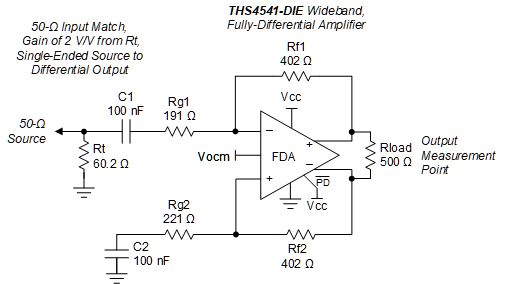
 Simplified Schematic
 Single to Differental Gain of 2,
2-V Output