SBOS831B December 2016 – June 2021 THS4552
PRODUCTION DATA
- 1 Features
- 2 Applications
- 3 Description
- 4 Revision History
- 5 Pin Configuration and Functions
-
6 Specifications
- 6.1 Absolute Maximum Ratings
- 6.2 ESD Ratings
- 6.3 Recommended Operating Conditions
- 6.4 Thermal Information
- 6.5 Electrical Characteristics: (VS+) – (VS–) = 5 V
- 6.6 Electrical Characteristics: (VS+) – (VS–) = 3 V
- 6.7 Typical Characteristics: (VS+) – (VS–) = 5 V
- 6.8 Typical Characteristics: (VS+) – (VS–) = 3 V
- 6.9 Typical Characteristics: 3 V to 5 V Supply Range
-
7 Parameter Measurement Information
- 7.1 Example Characterization Circuits
- 7.2 Output Interface Circuit for DC-Coupled Differential Testing
- 7.3 Output Common-Mode Measurements
- 7.4 Differential Amplifier Noise Measurements
- 7.5 Balanced Split-Supply Versus Single-Supply Characterization
- 7.6 Simulated Characterization Curves
- 7.7 Terminology and Application Assumptions
- 8 Detailed Description
-
9 Application and Implementation
- 9.1
Application Information
- 9.1.1 Noise Analysis
- 9.1.2 Factors Influencing Harmonic Distortion
- 9.1.3 Driving Capacitive Loads
- 9.1.4 Interfacing to High-Performance Precision ADCs
- 9.1.5 Operating the Power Shutdown Feature
- 9.1.6 Channel-to-Channel Crosstalk
- 9.1.7 Channel-to-Channel Mismatch
- 9.1.8 Designing Attenuators
- 9.1.9 The Effect of Adding a Feedback Capacitor
- 9.2 Typical Applications
- 9.1
Application Information
- 10Power Supply Recommendations
- 11Layout
- 12Device and Documentation Support
- 13Mechanical, Packaging, and Orderable Information
Package Options
Mechanical Data (Package|Pins)
Thermal pad, mechanical data (Package|Pins)
- RTW|24
Orderable Information
5 Pin Configuration and Functions
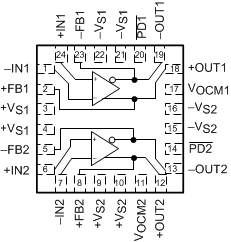
 Figure 5-1 RTW Package24-Pin VQFN With Exposed Thermal PadTop View
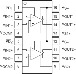
 Figure 5-2 PW Package16-Pin VSSOPTop View
Table 5-1 Pin Functions
| PIN | I/O | DESCRIPTION | ||
|---|---|---|---|---|
| NAME | NO. | |||
| RTW(1) | PW | |||
| FB1– | 23 | — | O | Channel 1, inverting (negative) output feedback |
| FB2– | 5 | — | O | Channel 2, inverting (negative) output feedback |
| FB1+ | 2 | — | O | Channel 1, noninverting (positive) output feedback |
| FB2+ | 8 | — | O | Channel 2, noninverting (positive) output feedback |
| IN1– | 1 | 3 | I | Channel 1, inverting (negative) amplifier input |
| IN2– | 7 | 7 | I | Channel 2, inverting (negative) amplifier input |
| IN1+ | 24 | 2 | I | Channel 1, noninverting (positive) amplifier input |
| IN2+ | 6 | 6 | I | Channel 2, noninverting (positive) amplifier input |
| OUT1– | 19 | 15 | O | Channel 1, inverting (negative) amplifier output |
| OUT2– | 13 | 11 | O | Channel 2, inverting (negative) amplifier output |
| OUT1+ | 18 | 14 | O | Channel 1, noninverting (positive) amplifier output |
| OUT2+ | 12 | 10 | O | Channel 2, noninverting (positive) amplifier output |
| PD1 | 20 | 1 | I | Channel 1, power-down. PD = logic low = power off mode; PD = logic high = normal operation. |
| PD2 | 14 | 5 | I | Channel 2, power-down. PD = logic low = power off mode; PD = logic high = normal operation. |
| VOCM1 | 17 | 4 | I | Channel 1, common-mode voltage input |
| VOCM2 | 11 | 8 | I | Channel 2, common-mode voltage input |
| VS1– | 21, 22 | 16 | I | Channel 1, negative power-supply input |
| VS2– | 15.16 | 12 | I | Channel 2, negative power-supply input |
| VS1+ | 3,4 | 13 | I | Channel 1, positive power-supply input |
| VS2+ | 9.10 | 9 | I | Channel 2, positive power-supply input |
(1) Solder the exposed thermal pad (RTW package) to a
heat-spreading power or ground plane. This pad is electrically isolated from the
die, but must be connected to a power or ground plane and not floated.