at TA ≈ 25°C, VOCM pin = open,
RF = 1 kΩ, RL = 1 kΩ, VOUT = 2 VPP,
50 Ω input match, G = 1 V/V, PD = VS+, single-ended
input, differential output, and input and output referenced to default midsupply for
ac-coupled tests (unless otherwise noted); see Figure 7-1 for a gain of 1 V/V test circuit
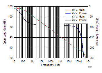
| Simulated with a 1 kΩ differential load and
0.6 pF internal feedback capacitors removed |
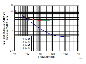 Figure 6-39 Input Spot Noise vs Frequency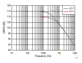
| Common-mode input to differential output, simulated with G = 1 V/V |
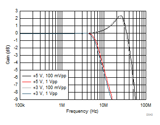 Figure 6-43 Common-Mode Voltage, Small- and Large-Signal Response (VOCM Pin
Driven)
Figure 6-43 Common-Mode Voltage, Small- and Large-Signal Response (VOCM Pin
Driven)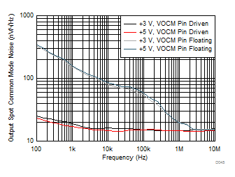
| The
VOCM pin is either driven to mid-supply by low-impedance
source or allowed to float and default to
mid-supply |
Figure 6-45 Output Common-Mode Noise vs Frequency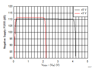
| Simulated with single-ended to differential gain of 1,
PSRR for negative supply to differential output |
Figure 6-47 –PSRR
vs VOCM Approaching VS–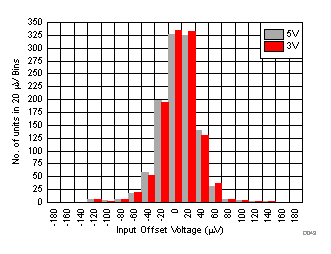
| Total of 561 PW units trimmed at a 5 V supply |
Figure 6-49 Input
Offset Voltage (VIO)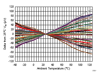
| 5 V
and 3 V delta from 25°C VIO, 52 PW
units |
Figure 6-51 Input
Offset Voltage vs Temperature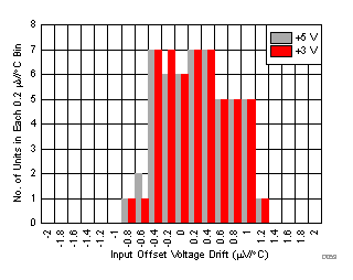
| –40°C to +125°C endpoint drift, total of 52 PW
units |
Figure 6-53 Input
Offset Voltage Drift Histogram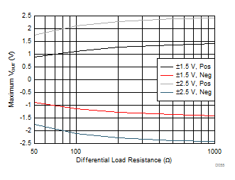
| Maximum differential output swing, VOCM at
mid-supply |
Figure 6-55 ±Maximum VOUT vs Differential Load Resistance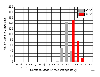
| VOCM input floating, total of 240
units |
Figure 6-57 Common-Mode Output Offset from VS+ / 2 Default Value
Histogram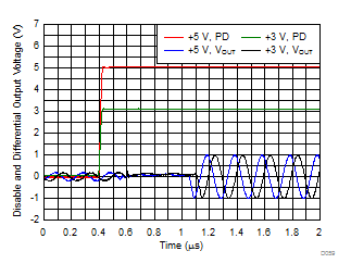 Figure 6-59 PD Turn-On Waveform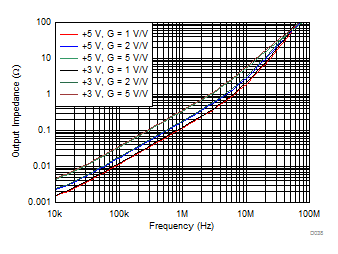
| Simulated closed-loop differential output impedance |
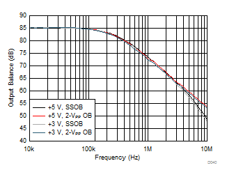
| Differential mode output to common-mode
output, simulated with G = 1 V/V Note: SSOB is equal to
a 20 mVPP output balance (OB). |
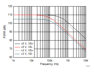
| Single-ended to differential gain of 1, PSRR simulated to differential output |
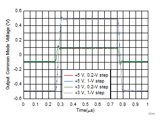 Figure 6-44 Common-Mode Voltage, Small- and Large-Step Response (VOCM Pin
Driven)
Figure 6-44 Common-Mode Voltage, Small- and Large-Step Response (VOCM Pin
Driven)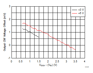
| Average VOCM output offset of 39 units,
standard deviation < 2 mV |
Figure 6-46 VOCM Offset vs VOCM Setting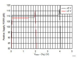
| Simulated with single-ended to differential gain of 1,
PSRR for positive supply to differential output |
Figure 6-48 +PSRR
vs VOCM Approaching VS+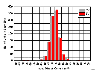
| Total of 561 PW units trimmed at a 5 V supply |
Figure 6-50 Input
Offset Current (IOS)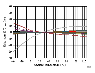
| 5 V
and 3 V delta from 25°C IOS, 52 PW
units |
Figure 6-52 Input
Offset Current vs Temperature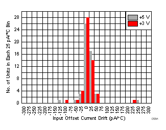
| –40°C to +125°C endpoint drift, total of 52 PW
units |
Figure 6-54 Input
Offset Current Drift Histogram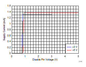 Figure 6-56 Supply Current vs PD Voltage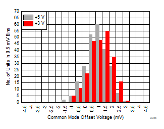
| VOCM input driven to mid-supply, total
of 240 units |
Figure 6-58 Common-Mode Output Offset from Driven VOCM Histogram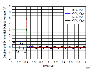 Figure 6-60 PD Turn-Off Waveform