SBOS643A April 2014 – May 2014 THS6226A
PRODUCTION DATA.
- 1 Features
- 2 Applications
- 3 Description
- 4 Revision History
- 5 Pin Configuration and Functions
- 6 Specifications
- 7 Detailed Description
- 8 Applications and Implementation
- 9 Power Supply Recommendations
- 10Layout
- 11Device and Documentation Support
- 12Mechanical, Packaging, and Orderable Information
Package Options
Mechanical Data (Package|Pins)
- RHB|32
Thermal pad, mechanical data (Package|Pins)
- RHB|32
Orderable Information
8 Applications and Implementation
8.1 Application Information
The device is a dual-port, very-high-bit-rate digital subscriber line (VDSL), class H line driver. Typically, the signal is generated by a high-speed digital-to-analog converter (DAC). The device drives a twisted pair.
The digital subscriber line (DSL) system is ac-coupled as it transmits information above the audio band. On the input of the line driver, this ac-coupling translates into the series capacitors to isolate the dc voltage coming from the DAC output common-mode voltage. On the output, a transformer is used to help isolate the 48V present between tip and ring of the telephone line.
The transformer can be set to any useful ratio. In practice, the transformer-turn ratio is set between 1:1 and 1:1.4 for the device. As mentioned in the Feature Description section, the active impedance synthesis factor is 5. This synthesis factor means that the termination resistor is 1/5th of the load impedance reflected to the transformer secondary. Thus, the correct termination can be selected based on the transformer-turn ratio.
Note that the resulting load detected by the amplifier may affect the amplifier linearity or output voltage swing capabilities.
8.2 Typical Application
The typical application circuit for this application is shown in Figure 34.
 Figure 34. Typical VDSL Line Driver Circuit Configuration
8.2.1 Design Requirements
Table 6. Design Requirements
| DESIGN REQUIREMENT | CONDITION |
|---|---|
| AC-coupling capacitors | 0.1 µF |
| Synthesis factor | 5 |
| Output transformer ratio | 1:1.4 |
| Surge protection circuit | Not shown |
8.2.2 Detailed Design Procedure
The input capacitor forms a high-pass filter with the device input impedance. This pole must be set at a frequency low enough to not interfere with the desired signal.
The output transformer can be changed to any transformer-turn ratio. Note that the load is expected to be a transmission line with 100-Ω characteristic impedance. Referred to the transformer secondary, the load detected by the amplifier is 1 / n2 with 1:n being the transformer-turn ratio.
Practical limitations force the transformer-turn ratio to be between 1.4:1 and 1:2. At the lighter load detected by the amplifier (1.4:1), the voltage swing is limited by the class H and the maximum achievable swing of the amplifier. At the heaviest load (1:2), the voltage swing is limited by the current drive capability of the amplifier. To satisfy the synthesis impedance factor and the loading, the series resistance (RS) can be set to RS = RL / 5 = 100 Ω / (5 × n2).
For the charge pump, consider the thermal characteristic of the capacitor (X7R, X5R, or Y5V can be used for the charge pump).
For the power-supply bypass, consider using only X7R or X5R because of the better stability of these materials over temperature.
For surge protection, consider adding 47-Ω resistors in series on the positive feedback path. The secondary protection is also normally added after the series resistance on the secondary transformer.
8.2.3 Application Curves
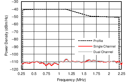
| 19.8-dBm Tx Power | Bias 2 | |
| 1:1.4 Transformer into 100 Ω | ||
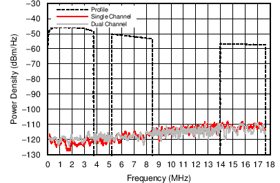
| 14.5-dBm Tx Power | Bias 11 | |||
| 1:1.4 Transformer into 100 Ω | ||||
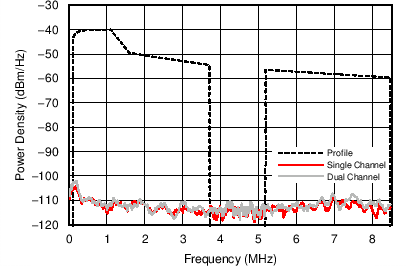
| 20.5-dBm Tx Power | Bias 7 | |
| 1:1.4 Transformer into 100 Ω | ||
8.3 Initialization Set Up
After the initial power-up and prior to sending any words to program the device, TI recommends sending a string of twelve 1s (111111111111) to ensure that the state machine is initialized.