SBOS643A April 2014 – May 2014 THS6226A
PRODUCTION DATA.
- 1 Features
- 2 Applications
- 3 Description
- 4 Revision History
- 5 Pin Configuration and Functions
- 6 Specifications
- 7 Detailed Description
- 8 Applications and Implementation
- 9 Power Supply Recommendations
- 10Layout
- 11Device and Documentation Support
- 12Mechanical, Packaging, and Orderable Information
Package Options
Mechanical Data (Package|Pins)
- RHB|32
Thermal pad, mechanical data (Package|Pins)
- RHB|32
Orderable Information
5 Pin Configuration and Functions
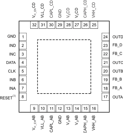
1. The PowerPAD is electrically isolated from all other pins and can be connected to any potential voltage range from VS– to VS+. Typically, the PowerPAD is connected to the GND plane because this plane tends to physically be the largest and is able to dissipate the most amount of heat.
2. The device defaults to the disabled mode at power-up.
3. Default is GND (internal pull-down resistor).
Pin Functions
| PIN | I/O | DESCRIPTION | |
|---|---|---|---|
| NO. | NAME | ||
| 1, 12, 29 | GND | — | Analog ground |
| 2 | IND | I | Input D of amplifier CD |
| 3 | INC | I | Input C of amplifier CD |
| 4 | DATA | I | Serial interface data pin |
| 5 | CLK | I | Serial interface CLK pin |
| 6 | INB | I | Input B of amplifier AB |
| 7 | INA | I | Input A of amplifier AB |
| 8 | RESET | I | Reset the internal register to 00h (startup conditions, state machine may require resetting) |
| 9 | VH_ENAB | I | Class H mode control pin for amplifier AB |
| 10 | VLL_AB | — | Amplifier AB low pump supply |
| 11 | CAPL_AB | — | Amplifier AB negative voltage pump capacitor pin |
| 13, 14 | VSAB | — | Amplifier AB supply voltage |
| 15 | CAPH_AB | — | Amplifier AB positive voltage pump capacitor pin |
| 16 | VHH_AB | — | Amplifier AB high pump supply |
| 17 | OUTA | O | Output A of amplifier AB |
| 18 | FB_A | I | Feedback for active output impedance of amplifier AB |
| 19 | FB_B | I | Feedback for active output impedance of amplifier AB |
| 20 | OUTB | O | Output B of amplifier AB |
| 21 | OUTC | O | Output C of amplifier CD |
| 22 | FB_C | I | Feedback for active output impedance of amplifier CD |
| 23 | FB_D | I | Feedback for active output impedance of amplifier CD |
| 24 | OUTD | O | Output D of amplifier CD |
| 25 | VHH_CD | — | Amplifier CD high pump supply |
| 26 | CAPH_CD | — | Amplifier CD positive voltage pump capacitor pin |
| 27, 28 | VSCD | — | Amplifier CD supply voltage |
| 30 | CAPL_CD | — | Amplifier CD negative voltage pump capacitor pin |
| 31 | VLL_CD | — | Amplifier CD low pump supply |
| 32 | VH_ENCD | I | Class H mode control pin for amplifier CD |
| PowerPAD | — | The PowerPAD must be connected to any internal PCB ground plane using multiple vias for good thermal performance. | |