SBOS643A April 2014 – May 2014 THS6226A
PRODUCTION DATA.
- 1 Features
- 2 Applications
- 3 Description
- 4 Revision History
- 5 Pin Configuration and Functions
- 6 Specifications
- 7 Detailed Description
- 8 Applications and Implementation
- 9 Power Supply Recommendations
- 10Layout
- 11Device and Documentation Support
- 12Mechanical, Packaging, and Orderable Information
Package Options
Mechanical Data (Package|Pins)
- RHB|32
Thermal pad, mechanical data (Package|Pins)
- RHB|32
Orderable Information
10 Layout
10.1 Layout Guidelines
Achieving optimum performance with a high-frequency amplifier such as the THS6226A requires careful attention to board layout parasitics and external component types. Recommendations that optimize performance include:
- Minimize parasitic capacitance to any ac ground for all signal I/O pins. Excessive parasitic capacitance on the inverting input pin can cause instability. In the line driver application, the parasitic capacitance forms a pole with the load detected by the amplifier and may reduce the effective bandwidth of the application circuit, thus leading to degraded performance. To reduce unwanted capacitance, open a window around the signal I/O pins in all ground and power planes around those pins. Otherwise, make sure that ground and power planes are unbroken elsewhere on the board.
- Minimize the distance (< 0.25") from the power-supply pins to high-frequency 0.1-µF decoupling capacitors. At the device pins, make sure that the ground and power-plane layout are not in close proximity to the signal I/O pins. Avoid narrow power and ground traces to minimize inductance between the pins and decoupling capacitors. Always decouple the power-supply connections with these capacitors. An additional low ESR supply decoupling capacitor (≥ 2 µF, X7R or X5R) to ground is necessary to provide a transient current during the charge pump capacitors recharge.
- Careful selection and placement of external components preserves the high-frequency performance of the device. Use very low reactance type resistors. Surface-mount resistors function best and allow a tighter overall layout. Metal-film or carbon composition, axially-leaded resistors also provide good high-frequency performance. Again, keep the leads and printed circuit board traces as short as possible. Never use wire-wound type resistors in a high-frequency application.
- Connections to other wideband devices on the board can be made with short, direct traces or through onboard transmission lines. For short connections, consider the trace and the input to the next device as a lumped capacitive load. Use relatively wide traces (50 mils to 100 mils), preferably with ground and power planes opened up around them.
- Do not socket a high-speed part such as the THS6226A. The additional lead length and pin-to-pin capacitance introduced by the socket can create an extremely troublesome parasitic network that makes achieving a smooth, stable frequency response almost impossible. Best results are obtained by soldering the device onto the board.
10.2 Layout Example
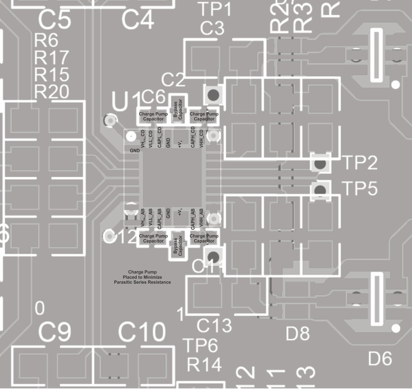 Figure 38. Layout Example