SCPS269 September 2017 TIC12400
PRODUCTION DATA.
- 1 Features
- 2 Applications
- 3 Description
- 4 Revision History
- 5 Pin Configuration and Functions
- 6 Specifications
- 7 Parameter Measurement Information
-
8 Detailed Description
- 8.1 Overview
- 8.2 Functional Block Diagram
- 8.3
Feature Description
- 8.3.1 VS Pin
- 8.3.2 VDD Pin
- 8.3.3 Device Initialization
- 8.3.4 Device Trigger
- 8.3.5 Device Reset
- 8.3.6 VS Under-Voltage (UV) Condition
- 8.3.7 VS Over-Voltage (OV) Condition
- 8.3.8 Switch inputs Settings
- 8.3.9 Interrupt Generation and INT Assertion
- 8.3.10 Temperature Monitor
- 8.3.11 Parity Check And Parity Generation
- 8.3.12 Cyclic Redundancy Check (CRC)
- 8.4 Device Functional Modes
- 8.5 Programming
- 8.6
Register Maps
- 8.6.1 DEVICE_ID register (Offset = 1h) [reset = 20h]
- 8.6.2 INT_STAT Register (Offset = 2h) [reset = 1h]
- 8.6.3 CRC Register (Offset = 3h) [reset = FFFFh]
- 8.6.4 IN_STAT_MISC Register (Offset = 4h) [reset = 0h]
- 8.6.5 IN_STAT_COMP Register (Offset = 5h) [reset = 0h]
- 8.6.6 IN_STAT_ADC0 Register (Offset = 6h) [reset = 0h]
- 8.6.7 IN_STAT_ADC1 Register (Offset = 7h) [reset = 0h]
- 8.6.8 IN_STAT_MATRIX0 Register (Offset = 8h) [reset = 0h]
- 8.6.9 IN_STAT_MATRIX1 Register (Offset = 9h) [reset = 0h]
- 8.6.10 ANA_STAT0 Register (Offset = Ah) [reset = 0h]
- 8.6.11 ANA_STAT1 Register (Offset = Bh) [reset = 0h]
- 8.6.12 ANA_STAT2 Register (Offset = Ch) [reset = 0h]
- 8.6.13 ANA_STAT3 Register (Offset = Dh) [reset = 0h]
- 8.6.14 ANA_STAT4 Register (Offset = Eh) [reset = 0h]
- 8.6.15 ANA_STAT5 Register (Offset = Fh) [reset = 0h]
- 8.6.16 ANA_STAT6 Register (Offset = 10h) [reset = 0h]
- 8.6.17 ANA_STAT7 Register (Offset = 11h) [reset = 0h]
- 8.6.18 ANA_STAT8 Register (Offset = 12h) [reset = 0h]
- 8.6.19 ANA_STAT9 Register (Offset = 13h) [reset = 0h]
- 8.6.20 ANA_STAT10 Register (Offset = 14h) [reset = 0h]
- 8.6.21 ANA_STAT11 Register (Offset = 15h) [reset = 0h]
- 8.6.22 ANA_STAT12 Register (Offset = 16h) [reset = 0h]
- 8.6.23 CONFIG Register (Offset = 1Ah) [reset = 0h]
- 8.6.24 IN_EN Register (Offset = 1Bh) [reset = 0h]
- 8.6.25 CS_SELECT Register (Offset = 1Ch) [reset = 0h]
- 8.6.26 WC_CFG0 Register (Offset = 1Dh) [reset = 0h]
- 8.6.27 WC_CFG1 Register (Offset = 1Eh) [reset = 0h]
- 8.6.28 CCP_CFG0 Register (Offset = 1Fh) [reset = 0h]
- 8.6.29 CCP_CFG1 Register (Offset = 20h) [reset = 0h]
- 8.6.30 THRES_COMP Register (Offset = 21h) [reset = 0h]
- 8.6.31 INT_EN_COMP1 Register (Offset = 22h) [reset = 0h]
- 8.6.32 INT_EN_COMP2 Register (Offset = 23h) [reset = 0h]
- 8.6.33 INT_EN_CFG0 Register (Offset = 24h) [reset = 0h]
- 8.6.34 INT_EN_CFG1 Register (Offset = 25h) [reset = 0h]
- 8.6.35 INT_EN_CFG2 Register (Offset = 26h) [reset = 0h]
- 8.6.36 INT_EN_CFG3 Register (Offset = 27h) [reset = 0h]
- 8.6.37 INT_EN_CFG4 Register (Offset = 28h) [reset = 0h]
- 8.6.38 THRES_CFG0 Register (Offset = 29h) [reset = 0h]
- 8.6.39 THRES_CFG1 Register (Offset = 2Ah) [reset = 0h]
- 8.6.40 THRES_CFG2 Register (Offset = 2Bh) [reset = 0h]
- 8.6.41 THRES_CFG3 Register (Offset = 2Ch) [reset = X]
- 8.6.42 THRES_CFG4 Register (Offset = 2Dh) [reset = X]
- 8.6.43 THRESMAP_CFG0 Register (Offset = 2Eh) [reset = 0h]
- 8.6.44 THRESMAP_CFG1 Register (Offset = 2Fh) [reset = 0h]
- 8.6.45 THRESMAP_CFG2 Register (Offset = 30h) [reset = 0h]
- 8.6.46 Matrix Register (Offset = 31h) [reset = 0h]
- 8.6.47 Mode Register (Offset = 32h) [reset = 0h]
- 8.7 Programming Guidelines
- 9 Application and Implementation
- 10Power Supply Recommendations
- 11Layout
- 12Device and Documentation Support
- 13Mechanical, Packaging, and Orderable Information
Package Options
Mechanical Data (Package|Pins)
- DCP|38
Thermal pad, mechanical data (Package|Pins)
- DCP|38
Orderable Information
9 Application and Implementation
NOTE
Information in the following applications sections is not part of the TI component specification, and TI does not warrant its accuracy or completeness. TI’s customers are responsible for determining suitability of components for their purposes. Customers should validate and test their design implementation to confirm system functionality.
9.1 Application Information
The TIC12400 is an advanced 24-input Multiple Switch Detection Interface (MSDI) device designed to detect external switch status and voltage levels by acting as an interface between the switches and the low- voltage microcontroller. The device offers a number of unique features to replace systems implemented with discrete components, providing board space savings and reduced bill of material (BOM). The device can also be configured into low-power polling mode, which provides significant savings on system power consumption. The TIC12400 is also suitable for many types of data acquisition systems with its integrated ADC, serialization, and digital communication capabilities.
9.2 Digital IO Switches and Analog Voltage Monitoring
The input stage of the TIC12400 is designed so that for an input resistance of 400 Ω on the IN0 - IN9 pins, the 10 mA current sink setting can be used for IEC61131-2 Type1, Type 2, and Type 3 switches.
Figure 82 depicts how the TIC12400 is used in a multiple purpose application with Digital IO Switches an analog sensor inputs using both the internal comparator and the ADC.
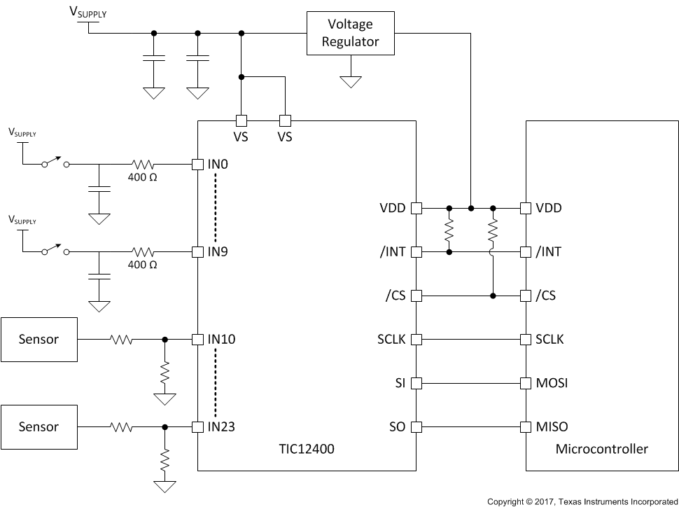 Figure 82. Using TIC12400 to Monitor digital IO switches and analog sensor inputs
9.2.1 Design Requirements
Table 60. Example Digital IO Switch Specification
| Specification | Min | Max | |
|---|---|---|---|
| VSUPPLY | 6.5 V ≤ VSUPPLY ≤ 18 V | 6.5 V | 18 V |
| RIN | 400 Ω ± 10% | 360 Ω | 440 Ω |
| ISINK | 10 mA | 9.2 mA | 13.4 mA |
9.2.2 Detailed Design Procedure
For digital I/O applications, the inputs must be connected to the IN0 - IN9 pins as these are the only inputs that have the current sink necessary to facilitate these type of switches. The external resistor must be sized so that the pin voltage VINX remains below the max comparator threshold of 4.7 V until the current sink is saturated by the pin voltage. This ensures a low will always be considered a low as the external system voltage VIN continues to increase. Lower comparator voltages can be used if the external components are sized to ensure that until the current sink is saturated, the voltage remains below the comparator threshold.
To select the resistor for a digital I/O application, ensure the voltage on the INX pin (IN0 - IN9) remains below the comparator threshold until the input voltage VIN is above the OFF region defined by the IEC standard. With a 400-Ω resistor and worst case current of 9.2 mA, a 3.68 V voltage drop is observer across the resistor. This keeps the VINX 3.68 V below the system input VIN, ensuring that comparator does not detect a high until VIN is out of the OFF region and in the ON region.
The second use case for TIC12400 is to monitor analog input voltages from external sensors. These sensors could be a high or low type sensor that has a 1 or 0 representation of the output. In this case, the comparator mode of the input can be used. To ensure correct operation, a voltage divider may be necessary to scale the incoming voltage so that a low will be below the chosen comparator threshold. For reference the available comparator thresholds are 2 V, 2.7 V, 3 V, and 4 V.
For multi level sensor outputs the TIC12400 internal ADC can be used to set to monitor analog input voltages. The following procedure can be used to setup the TIC12400 ADC inputs
- The first step is to set any input that will be used in a pure analog ADC mode to the 0 mA current setting.
- The second step is to estimate the voltage output of the sensor. The full-scale range of the 10-bit ADC is from 0 V to 6 V, with 6 V corresponding to the max code of 1023. A resistor divider can be used to scale the input voltage to meet this requirement by using VIN = VSENSOR_OUTPUT x R1/(R1+ R2) = 6 V max.
- The next step is to determine if a wake up feature is needed that uses the ADC thresholds. This could be used to wake up the system in the case that a temperature sensor has indicated a potentially damaging temperature that requires system interaction to fix. The TIC12400 can handle two input states on inputs IN0 - IN11, three input states on inputs IN12 - IN17, 4 input states on IN18 - IN22 and 6 input states on IN 23. Every threshold crossing can trigger an interrupt if required by the system. If no interrupt triggers are needed move on to step three.
- After the measurement is taken, the raw ADC code will be stored in the ANA_STAT registers to be read by the host for interpretation.
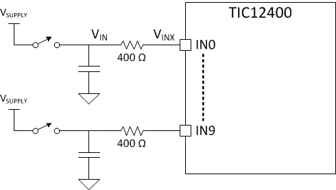 Figure 83. Digital IO Switch Input Example
9.2.3 Application Curves
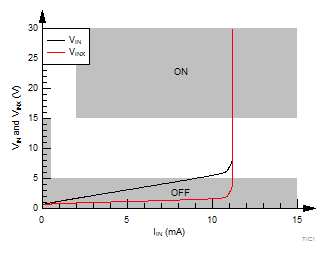 Figure 84. Type-1 Switch with 400-Ω Input Resistor
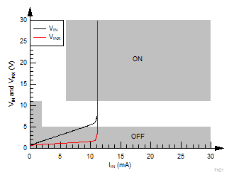 Figure 85. Type-2 Switch with 400-Ω Input Resistor
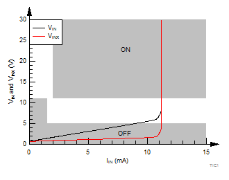 Figure 86. Type-3 Switch with 400-Ω Input Resistor