SLVS543R August 2004 – October 2023 TL431 , TL432
PRODUCTION DATA
- 1
- 1 Features
- 2 Applications
- 3 Description
- 4 Revision History
- 5 Device Comparison Table
- 6 Pin Configuration and Functions
-
7 Specifications
- 7.1 Absolute Maximum Ratings
- 7.2 ESD Ratings
- 7.3 Thermal Information
- 7.4 Recommended Operating Conditions
- 7.5 Electrical Characteristics, TL431C, TL432C
- 7.6 Electrical Characteristics, TL431I, TL432I
- 7.7 Electrical Characteristics, TL431Q, TL432Q
- 7.8 Electrical Characteristics, TL431AC, TL432AC
- 7.9 Electrical Characteristics, TL431AI, TL432AI
- 7.10 Electrical Characteristics, TL431AQ, TL432AQ
- 7.11 Electrical Characteristics, TL431BC, TL432BC
- 7.12 Electrical Characteristics, TL431BI, TL432BI
- 7.13 Electrical Characteristics, TL431BQ, TL432BQ
- 7.14 Typical Characteristics
- 8 Parameter Measurement Information
- 9 Detailed Description
- 10Applications and Implementation
- 11Device and Documentation Support
- 12Mechanical, Packaging, and Orderable Information
Package Options
Mechanical Data (Package|Pins)
Thermal pad, mechanical data (Package|Pins)
- PK|3
Orderable Information
10.3 System Examples
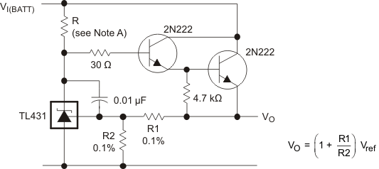
A. R should provide cathode current ≥1 mA to the TL431 at minimum V(BATT).
Figure 10-5 Precision High-Current Series Regulator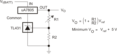 Figure 10-6 Output Control of a Three-Terminal Fixed Regulator
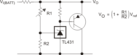 Figure 10-7 High-Current Shunt Regulator
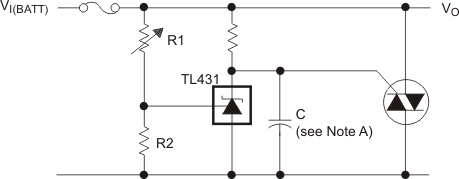
A. Refer to the stability boundary conditions in Figure 7-16 and Figure 7-18 to determine allowable values for C.
Figure 10-8 Crowbar Circuit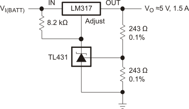 Figure 10-9 Precision 5-V, 1.5-A Regulator
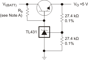
A. Rb should provide cathode current ≥1 mA to the TL431.
Figure 10-10 Efficient 5-V Precision Regulator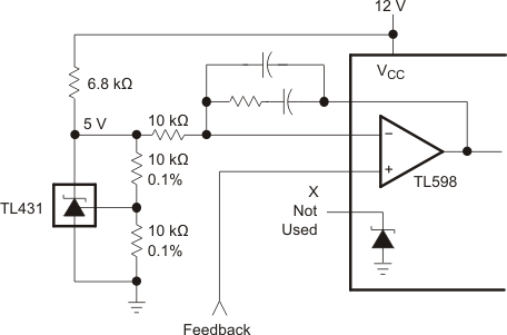 Figure 10-11 PWM Converter With Reference
A. Select R3 and R4 to provide the desired LED intensity and cathode current ≥1 mA to the TL431 at the available VI(BATT).
Figure 10-12 Voltage Monitor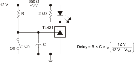 Figure 10-13 Delay Timer
 Figure 10-14 Precision Current Limiter
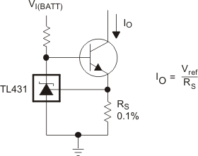 Figure 10-15 Precision Constant-Current Sink