SLOS154C December 1995 – July 2025 TLC27L1 , TLC27L1A
PRODUCTION DATA
- 1
- 1 Features
- 2 Applications
- 3 Description
- 4 Pin Configuration and Functions
-
5 Specifications
- 5.1 Absolute Maximum Ratings
- 5.2 Dissipation Ratings
- 5.3 Recommended Operating Conditions
- 5.4 Electrical Characteristics, C Suffix
- 5.5 Operating Characteristics, VDD = 5V, C Suffix
- 5.6 Operating Characteristics, VDD = 10V, C Suffix
- 5.7 Electrical Characteristics, I Suffix
- 5.8 Operating Characteristics, VDD = 5V, I Suffix
- 5.9 Operating Characteristics, VDD = 10V, I Suffix
- 5.10 Typical Characteristics
- 6 Parameter Measurement Information
- 7 Application and Implementation
- 8 Device and Documentation Support
- 9 Revision History
- 10Mechanical, Packaging, and Orderable Information
Package Options
Refer to the PDF data sheet for device specific package drawings
Mechanical Data (Package|Pins)
- D|8
- P|8
Thermal pad, mechanical data (Package|Pins)
Orderable Information
7.1.1 Single-Supply Operation
While the TLC27L1 performs well using dual power supplies (also called balanced or split supplies), the design is optimized for single-supply operation. This optimization includes an input common-mode voltage range that encompasses ground as well as an output voltage range that pulls down to ground. The supply voltage range extends down to 3V (C-suffix types), thus allowing operation with supply levels commonly available for TTL and HCMOS. For maximum dynamic range, 16V single-supply operation is recommended.
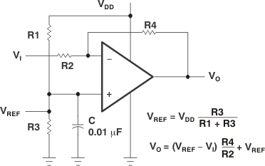
 Figure 7-1 Inverting
Amplifier With Voltage Reference
Figure 7-1 Inverting
Amplifier With Voltage ReferenceMany single-supply applications require that a voltage be applied to one input to establish a reference level that is above ground. A resistive voltage divider is typically sufficient to establish this reference level (see Figure 7-1). The low-input bias-current consumption of the TLC27L1 permits the use of very large resistive values to implement the voltage divider, thus minimizing power consumption.
The TLC27L1 works well in conjunction with digital logic; however, when powering both linear devices and digital logic from the same power supply, take the following recommended precautions:
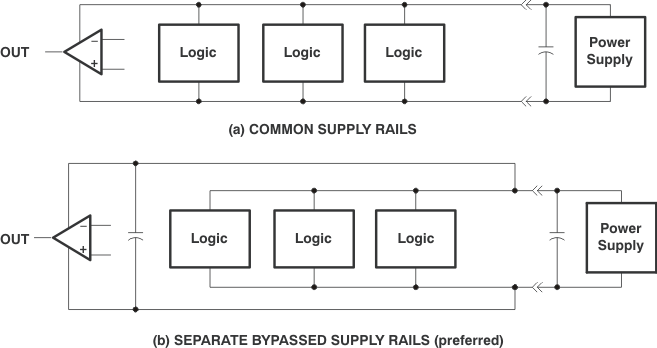
- Power linear devices from separate bypassed supply lines (see Figure 7-2); otherwise, linear device supply rails potentially fluctuate as a result of voltage drops caused by high switching currents in the digital logic.
- Use proper bypass techniques to reduce the probability of noise-induced errors. Single capacitive decoupling is often adequate; however, RC decoupling is probably necessary in high-frequency applications.
 Figure 7-2 Common
Versus Separate Supply Rails