SLOS154C December 1995 – July 2025 TLC27L1 , TLC27L1A
PRODUCTION DATA
- 1
- 1 Features
- 2 Applications
- 3 Description
- 4 Pin Configuration and Functions
-
5 Specifications
- 5.1 Absolute Maximum Ratings
- 5.2 Dissipation Ratings
- 5.3 Recommended Operating Conditions
- 5.4 Electrical Characteristics, C Suffix
- 5.5 Operating Characteristics, VDD = 5V, C Suffix
- 5.6 Operating Characteristics, VDD = 10V, C Suffix
- 5.7 Electrical Characteristics, I Suffix
- 5.8 Operating Characteristics, VDD = 5V, I Suffix
- 5.9 Operating Characteristics, VDD = 10V, I Suffix
- 5.10 Typical Characteristics
- 6 Parameter Measurement Information
- 7 Application and Implementation
- 8 Device and Documentation Support
- 9 Revision History
- 10Mechanical, Packaging, and Orderable Information
Package Options
Refer to the PDF data sheet for device specific package drawings
Mechanical Data (Package|Pins)
- D|8
- P|8
Thermal pad, mechanical data (Package|Pins)
Orderable Information
7.1.7 Output Characteristics
The output stage of the TLC27L1 is designed to sink and source relatively high amounts of current (see also Section 5.10). If the output is subjected to a short-circuit condition, the high-current capability is able to cause device damage under certain conditions. Output current capability increases with supply voltage (see Figure 7-7).
 Figure 7-7 Test Circuit for Output Characteristics
All operating characteristics of the TLC27L1 were measured using a 20pF load. The devices drive higher capacitive loads. However, as output load capacitance increases, the resulting response pole occurs at lower frequencies, thereby causing ringing, peaking, or even oscillation (see Figure 7-8). In many cases, adding some compensation in the form of a series resistor in the feedback loop alleviates the problem.
 Figure 7-8 Effect of Capacitive Loads in Low-Bias Mode
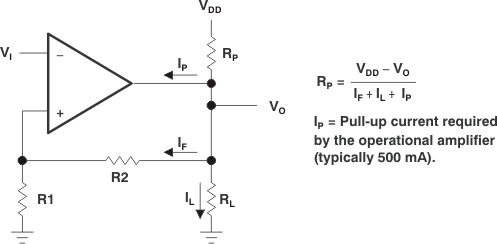
Although the TLC27L1 possesses excellent high-level output voltage and current capability, methods are available for boosting this capability, if needed. The simplest method involves the use of a pullup resistor (RP) connected from the output to the positive supply rail (see Figure 7-9). There are two disadvantages to using this circuit. First, the NMOS pulldown transistor must sink a comparatively large amount of current. In this circuit, the pulldown transistor behaves like a linear resistor with an on-resistance between approximately 60Ω and 180Ω, depending on how hard the operational amplifier input is driven. With very low values of RP, a voltage offset from 0V at the output occurs. Secondly, pullup resistor RP acts as a drain load to the pulldown resistor, and the gain of the operational amplifier is reduced at output voltage levels where the corresponding pullup resistor is not supplying the output current.
 Figure 7-9 Resistive Pullup Resistor
to Increase VOH