SBVS199C June 2012 – January 2024 TLC59283
PRODUCTION DATA
- 1
- 1 Features
- 2 Applications
- 3 Description
- 4 Pin Configurations
- 5 Specifications
- 6 Parameter Measurement Information
- 7 Detailed Description
- 8 Register Configuration
- 9 Application and Implementation
- 10Device and Documentation Support
- 11Revision History
- 12Mechanical, Packaging, and Orderable Information
Package Options
Mechanical Data (Package|Pins)
Thermal pad, mechanical data (Package|Pins)
Orderable Information
8 Register Configuration
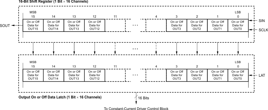
The TLC59283 has a 16-bit shift register and an output on or off data latch. Both the shift register and data latch are 16 bits long and are used to turn the constant-current outputs on and off. Figure 8-1 shows the shift register and data latch configuration. The data at the SIN pin are shifted into the 16-bit shift register LSB at the rising edge of the SCLK pin; SOUT data change at the SCLK rising edge.
 Figure 8-1 16-Bit Shift Register and Output On or Off Data Latch Configuration
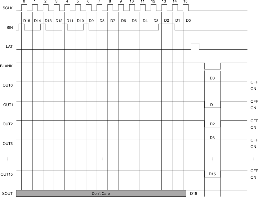
The output on or off data in the 16-bit shift register continue to transfer to the output on or off data latch while LAT is high. Therefore, if the data in the 16-bit shift register are changed when LAT is high, the data in the data latch are also changed. The data in the data latch are held when LAT is low. When the device initially powers on, the data in the output on or off shift register and latch are not set to default values; on or off control data must be written to the on or off control data latch before turning the constant-current output on. All constant-current outputs are forced off when BLANK is high. The OUTn on or off outputs are controlled by the data in the output on or off data latch. The writing data truth table and timing diagram are shown in Table 8-1 and Figure 8-2, respectively.
| SCLK | LAT | BLANK | SIN | OUT0…OUT7…OUT15 | SOUT |
|---|---|---|---|---|---|
| ↑ | High | Low | Dn | Dn…Dn – 7…Dn – 15 | Dn – 15 |
| ↑ | Low | Low | Dn + 1 | No change | Dn – 14 |
| ↑ | High | Low | Dn + 2 | Dn + 2…Dn – 5…Dn – 13 | Dn – 13 |
| ↓ | — | Low | Dn + 3 | Dn + 2…Dn – 5…Dn – 13 | Dn – 13 |
| ↓ | — | High | Dn + 3 | Off | Dn – 13 |
 Figure 8-2 Operation Timing Diagram