SLLSFG0B November 2019 – May 2022 TLIN1028S-Q1
PRODUCTION DATA
- 1 Features
- 2 Applications
- 3 Description
- 4 Revision History
- 5 Description (continued)
- 6 Pin Configuration and Functions
- 7 Specification
- 8 Parameter Measurement Information
-
9 Detailed Description
- 9.1 Overview
- 9.2 Functional Block Diagram
- 9.3 Feature Description
- 9.4 Device Functional Modes
- 10Application and Implementation
- 11Power Supply Recommendations
- 12Layout
- 13Device and Documentation Support
- 14Mechanical, Packaging, and Orderable Information
Package Options
Mechanical Data (Package|Pins)
- D|8
Thermal pad, mechanical data (Package|Pins)
Orderable Information
9.4 Device Functional Modes
nRST: Float
nRST: Float
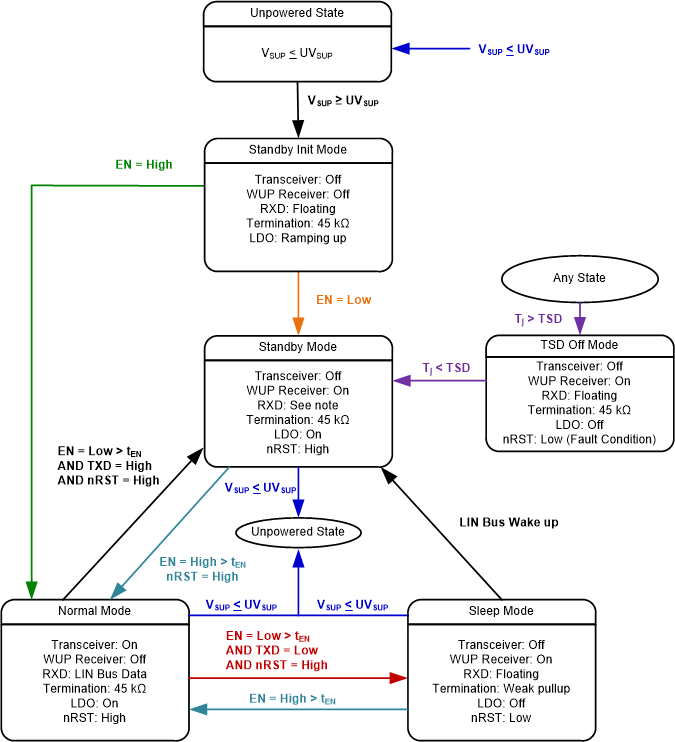
The TLIN1028S-Q1 has three functional modes of operation: normal, sleep, and standby. The next sections describes these modes as well as how the device moves between the different modes. Figure 9-5 graphically shows the relationship while Table 9-1 shows the state of pins.
Table 9-1 Operating Modes
| Mode | EN | RXD | LIN BUS Termination | Transmitter | nRST | Comment |
|---|---|---|---|---|---|---|
| Sleep | Low | Floating | Weak Current pull-up | Off | Ground | nRST is internally connected to the LDO output which is pulled to ground in sleep mode. |
| Standby Init | Low | Floating | 45 kΩ (typical) | Off | Ramping | nRST is internally connected to the LDO output which in standby init mode is pulled low until VCC raises beyond UVCC threshold. |
| Standby from SLP | Low | Low | 45 kΩ (typical) | Off | VCC | Wake-up event detected, waiting on processors to set EN nRST comes on to VCC once thresholds are met. |
| Standby from Norm | Low | High | 45 kΩ (typical) | Off | VCC | LDO is on and RXD is high |
| Normal | High | LIN Bus Data | 45 kΩ (typical) | On | VCC | LIN transmission up to 20 kbps |
| TSD Off | NA | Floating | 45 kΩ (typical) | Off | Ground | nRST is pulled low as the LDO is turned off which means UVCC threshold has been met. |
 Figure 9-5 Operating State Diagram
Note:
- RXD is latched low due to a wake event from sleep mode once entering standby mode
- RXD is high when entering standby mode from other modes and is not latch low for a wake event