SBOS784C November   2016  – January 2019 TLV172 , TLV2172 , TLV4172

PRODUCTION DATA.  

  1. Features
  2. Applications
  3. Description
    1.     Simplified Schematic
  4. Revision History
  5. Device Comparison Table
  6. Pin Configuration and Functions
    1.     Pin Functions: TLV172
    2.     Pin Functions: TLV2172
    3.     Pin Functions: TLV4172
  7. Specifications
    1. 7.1 Absolute Maximum Ratings
    2. 7.2 ESD Ratings
    3. 7.3 Recommended Operating Conditions
    4. 7.4 Thermal Information: TLV172
    5. 7.5 Thermal Information: TLV2172
    6. 7.6 Thermal Information: TLV4172
    7. 7.7 Electrical Characteristics
    8. 7.8 Typical Characteristics
  8. Detailed Description
    1. 8.1 Overview
    2. 8.2 Functional Block Diagram
    3. 8.3 Feature Description
      1. 8.3.1 Operating Characteristics
      2. 8.3.2 Phase-Reversal Protection
      3. 8.3.3 Electrical Overstress
      4. 8.3.4 Capacitive Load and Stability
    4. 8.4 Device Functional Modes
      1. 8.4.1 Common-Mode Voltage Range
      2. 8.4.2 Overload Recovery
  9. Application and Implementation
    1. 9.1 Application Information
    2. 9.2 Typical Application
      1. 9.2.1 Design Requirements
      2. 9.2.2 Detailed Design Procedure
      3. 9.2.3 Application Curve
  10. 10Power Supply Recommendations
  11. 11Layout
    1. 11.1 Layout Guidelines
    2. 11.2 Layout Example
  12. 12Device and Documentation Support
    1. 12.1 Device Support
      1. 12.1.1 Third-Party Products Disclaimer
      2. 12.1.2 Development Support
        1. 12.1.2.1 TINA-TI™ (Free Software Download)
        2. 12.1.2.2 DIP Adapter EVM
        3. 12.1.2.3 Universal Op Amp EVM
        4. 12.1.2.4 TI Precision Designs
        5. 12.1.2.5 WEBENCH Filter Designer
    2. 12.2 Documentation Support
      1. 12.2.1 Related Documentation
    3. 12.3 Related Links
    4. 12.4 Receiving Notification of Documentation Updates
    5. 12.5 Community Resources
    6. 12.6 Trademarks
    7. 12.7 Electrostatic Discharge Caution
    8. 12.8 Glossary
  13. 13Mechanical, Packaging, and Orderable Information

Package Options

Mechanical Data (Package|Pins)
Thermal pad, mechanical data (Package|Pins)
Orderable Information

Typical Application

This circuit can drive capacitive loads (such as cable shields, reference buffers, MOSFET gates, and diodes). The circuit uses an isolation resistor (RISO) to stabilize the output of an operational amplifier. RISO modifies the open-loop gain of the system to ensure that the circuit has sufficient phase margin.
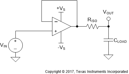
TLV172 TLV2172 TLV4172 refdes_blocldia_sbos782.gifFigure 29. Unity-Gain Buffer With RISO Stability Compensation