SNOSD52B August   2018  – January 2020 TLV1805-Q1

PRODUCTION DATA.  

  1. Features
  2. Applications
  3. Description
    1.     Device Images
      1.      Reverse Current Protection Using an N-Channel MOSFET
      2.      Reverse Current & Overvoltage Protection Using P-Channel MOSFETs
  4. Revision History
  5. Pin Configuration and Functions
    1.     Pin Functions
  6. Specifications
    1. 6.1 Absolute Maximum Ratings
    2. 6.2 ESD Ratings
    3. 6.3 Recommended Operating Conditions
    4. 6.4 Thermal Information
    5. 6.5 Electrical Characteristics
    6. 6.6 Switching Characteristics
    7. 6.7 Typical Characteristics
  7. Detailed Description
    1. 7.1 Overview
    2. 7.2 Functional Block Diagram
    3. 7.3 Feature Description
      1. 7.3.1 Rail to Rail Inputs
      2. 7.3.2 Power On Reset
      3. 7.3.3 High Power Push-Pull Output
      4. 7.3.4 Shutdown Function
      5. 7.3.5 Internal Hysteresis
    4. 7.4 Device Functional Modes
      1. 7.4.1 External Hysteresis
        1. 7.4.1.1 Inverting Comparator With Hysteresis
        2. 7.4.1.2 Noninverting Comparator With Hysteresis
  8. Application and Implementation
    1. 8.1 Application Information
    2. 8.2 Typical Applications
      1. 8.2.1 Design Requirements
      2. 8.2.2 Detailed Design Procedure
      3. 8.2.3 Application Curve
      4. 8.2.4 Reverse Current Protection Using MOSFET and TLV1805-Q1
        1. 8.2.4.1 Minimum Reverse Current
        2. 8.2.4.2 N-Channel Reverse Current Protection Circuit
          1. 8.2.4.2.1 N-Channel Oscillator Circuit
      5. 8.2.5 P-Channel Reverse Current Protection Circuit
      6. 8.2.6 P-Channel Reverse Current Protection With Overvotlage Protection
      7. 8.2.7 ORing MOSFET Controller
  9. Power Supply Recommendations
  10. 10Layout
    1. 10.1 Layout Guidelines
    2. 10.2 Layout Example
  11. 11Device and Documentation Support
    1. 11.1 Documentation Support
      1. 11.1.1 Related Documentation
    2. 11.2 Receiving Notification of Documentation Updates
    3. 11.3 Support Resources
    4. 11.4 Trademarks
    5. 11.5 Electrostatic Discharge Caution
    6. 11.6 Glossary
  12. 12Mechanical, Packaging, and Orderable Information

Package Options

Mechanical Data (Package|Pins)
Thermal pad, mechanical data (Package|Pins)
Orderable Information

ORing MOSFET Controller

The previous reverse current circuits may be combined to create an OR'ing supply controller, utilizing either the P-Channel or N-Channel topologies.

For the previous P-Channel circuit, if no negative input voltages are possible, and the input voltage is below the MOSFET's VGS(MAX) , then D3, D4 and R4 may be eliminated (the D2 anode, U1 pins 2 and 5, and C1 can be directly grounded).

For the N-Channel circuit, the oscillator drive can be shared between the channels, or eliminated if a higher system voltage is available to provide the higher votlage.
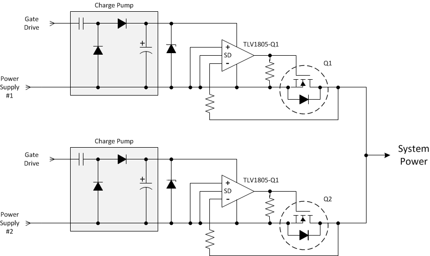
TLV1805-Q1 ORing_Q1.gifFigure 72. N-Channel OR'ing MOSFET Controller