SGLS008G March 2003 – February 2018 TLV2460A-Q1 , TLV2461A-Q1 , TLV2462-Q1 , TLV2462A-Q1 , TLV2463A-Q1 , TLV2464A-Q1
PRODUCTION DATA.
- 1 Features
- 2 Applications
- 3 Description
- 4 Revision History
- 5 Pin Configuration and Functions
-
6 Specifications
- 6.1 Absolute Maximum Ratings
- 6.2 ESD Ratings
- 6.3 Recommended Operating Conditions
- 6.4 Thermal Information: TLV2460x-Q1
- 6.5 Thermal Information: TLV2461x-Q1
- 6.6 Thermal Information: TLV2462-Q1
- 6.7 Thermal Information: TLV2462A-Q1
- 6.8 Thermal Information: TLV2463x-Q1
- 6.9 Electrical Characteristics: VDD = 3 V
- 6.10 Electrical Characteristics: VDD = 5 V
- 6.11 Operating Characteristics: VDD = 3 V
- 6.12 Operating Characteristics: VDD = 5 V
- 6.13 Typical Characteristics
- 7 Parameter Measurement Information
- 8 Detailed Description
- 9 Application and Implementation
- 10Power Supply Recommendations
- 11Layout
- 12Device and Documentation Support
- 13Mechanical, Packaging, and Orderable Information
Package Options
Refer to the PDF data sheet for device specific package drawings
Mechanical Data (Package|Pins)
- PW|8
Thermal pad, mechanical data (Package|Pins)
Orderable Information
9.1.1 Macromodel Information
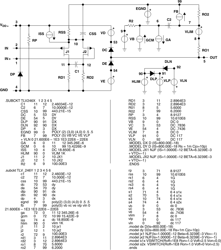
Macromodel information provided was derived using Microsim Parts™ Release 8, the model generation software used with Microsim PSpice™. The Boyle macromodel (1) and subcircuit in Figure 54 are generated using the TLV246x-Q1 typical electrical and operating characteristics at TA = 25°C. Using this information, output simulations of the following key parameters are generated to a tolerance of 20% (in most cases):
1. G. R. Boyle, B. M. Cohn, D. O. Pederson, and J. E. Solomon, “Macromodeling of Integrated Circuit Operational Amplifiers,” IEEE Journal of Solid-State Circuits, SC-9, 353 (1974).
- Maximum positive output voltage swing
- Maximum negative output voltage swing
- Slew rate
- Quiescent power dissipation
- Input bias current
- Open-loop voltage amplification
- Unity gain frequency
- Common-mode rejection ratio
- Phase margin
- DC output resistance
- AC output resistance
- Short-circuit output current limit
 Figure 54. Boyle Macromodel and Sub-Circuit