SLOS351E February 2004 – November 2016 TLV271 , TLV272 , TLV274
PRODUCTION DATA.
- 1 Features
- 2 Applications
- 3 Description
- 4 Revision History
- 5 Device Comparison Table
- 6 Pin Configuration and Functions
-
7 Specifications
- 7.1 Absolute Maximum Ratings
- 7.2 Recommended Operating Conditions
- 7.3 Thermal Information: TLV271
- 7.4 Thermal Information: TLV272
- 7.5 Thermal Information: TLV274
- 7.6 Electrical Characteristics: DC Characteristics
- 7.7 Electrical Characteristics: Input Characteristics
- 7.8 Electrical Characteristics: Output Characteristics
- 7.9 Electrical Characteristics: Power Supply
- 7.10 Electrical Characteristics: Dynamic Performance
- 7.11 Electrical Characteristics: Noise/Distortion Performance
- 7.12 Typical Characteristics
- 8 Detailed Description
- 9 Application and Implementation
- 10Power Supply Recommendations
- 11Layout
- 12Device and Documentation Support
- 13Mechanical, Packaging, and Orderable Information
Package Options
Refer to the PDF data sheet for device specific package drawings
Mechanical Data (Package|Pins)
- D|14
- PW|14
- N|14
Thermal pad, mechanical data (Package|Pins)
Orderable Information
8 Detailed Description
8.1 Overview
The TLV27x operates from a single power supply and consumes only 550 µA of quiescent current. With rail-to-rail output swing capability and 3-MHz bandwidth, the TLV27x is ideal for battery-powered and industrial applications.
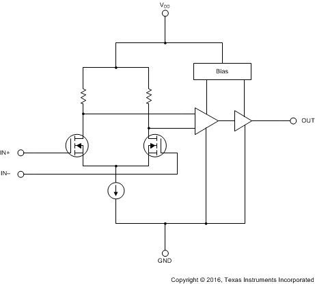
8.2 Functional Block Diagram

8.3 Feature Description
8.3.1 Rail to Rail Output
The TLV27x family of opamps features a rail to trail output stage. Rail to rail outputs allow for a wide dynamic range in low voltage systems. This feature along with low power and wide bandwidth make the TLV27x family suitable for portable and battery powered systems.
8.3.2 Offset Voltage
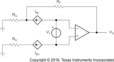
The output offset voltage (VOO) is the sum of the input offset voltage (VIO) and both input bias currents (IIB) times the corresponding gains. Use the schematic in Figure 25 and Equation 1 to calculate the output offset voltage:
 Figure 25. Output Offset Voltage Model

8.3.3 Driving a Capacitive Load
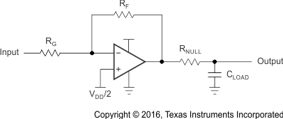
When the amplifier is configured in this manner, capacitive loading directly on the output decreases the device phase margin, leading to high frequency ringing or oscillations. Therefore, for capacitive loads of greater than 10 pF, TI recommends placing a resistor in series (RNULL) with the output of the amplifier, as shown in Figure 26. A minimum value of 20 Ω should work well for most applications.
 Figure 26. Driving a Capacitive Load
8.4 Device Functional Modes
The TLV27x has a single functional mode. It is operational when the power supply applied to the device is between 2.7 V (±1.35 V) and 16 V (±8 V). Electrical parameters that can vary with operating conditions are shown in Typical Characteristics.