SLAS520E February 2007 – December 2014 TLV320AIC3101
PRODUCTION DATA.
- 1 Features
- 2 Applications
- 3 Description
- 4 Simplified Diagram
- 5 Revision History
- 6 Description (continued)
- 7 Device Comparison Table
- 8 Pin Configuration and Functions
- 9 Specifications
- 10Parameter Measurement Information
-
11Detailed Description
- 11.1 Overview
- 11.2 Functional Block Diagram
- 11.3
Feature Description
- 11.3.1 Hardware Reset
- 11.3.2 Digital Audio Data Serial Interface
- 11.3.3 Audio Data Converters
- 11.3.4 Audio Analog Inputs
- 11.3.5 Analog Fully Differential Line Output Drivers
- 11.3.6 Analog High-Power Output Drivers
- 11.3.7 Input Impedance and VCM Control
- 11.3.8 MICBIAS Generation
- 11.3.9 Short-Circuit Output Protection
- 11.3.10 Jack/Headset Detection
- 11.4 Device Functional Modes
- 11.5 Programming
- 11.6 Register Maps
- 11.7 Output Stage Volume Controls
- 12Application and Implementation
- 13Power Supply Recommendations
- 14Layout
- 15Device and Documentation Support
- 16Mechanical, Packaging, and Orderable Information
Package Options
Mechanical Data (Package|Pins)
- RHB|32
Thermal pad, mechanical data (Package|Pins)
- RHB|32
Orderable Information
12 Application and Implementation
NOTE
Information in the following applications sections is not part of the TI component specification, and TI does not warrant its accuracy or completeness. TI’s customers are responsible for determining suitability of components for their purposes. Customers should validate and test their design implementation to confirm system functionality.
12.1 Application Information
The TLV320AIC3101 is a highly integrated low-power stereo audio codec with integrated stereo speaker/headphone/ line amplifier, as well as multiple inputs and outputs that are programmable in single-ended or fully differential configurations. Pairs of high power drivers can be used to drive 8-Ω speakers in BTL configuration. All the features of the TLV320AIC3101 are accessed by programmable registers. External processor with I2C protocol is required to control the device. It is good practice to perform a hardware reset after initial power up to ensure that all registers are in their default states. Extensive register-based power control is included, enabling stereo 48-kHz DAC playback as low as 14-mW from a 3.3-V analog supply, making it ideal for portable battery-powered audio and telephony applications.
12.2 Typical Application
12.2.1 AC-Coupled Headphone Output With Separate Line Outputs and External Speaker Amplifier
TLV320AIC3101 is a versatile device capable of being configured in several ways suited for portable applications. This device could be configured to have two microphones with an FM tuner connected to the analog inputs. High power driver outputs can drive an external power amplifier and headphone, and still have a fully differential stereo line output.
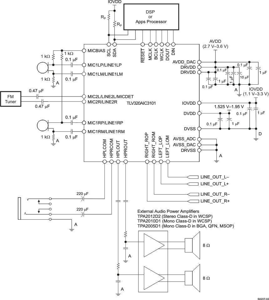 Figure 33. Typical Connections for AC-Coupled Headphone Output With Separate Line Outputs and External Speaker Amplifier
12.2.1.1 Design Requirements
For this design example, use the parameters shown in Table 180.
Table 180. Design Parameters
| PARAMETER | VALUE |
|---|---|
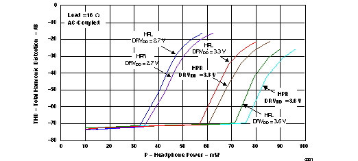
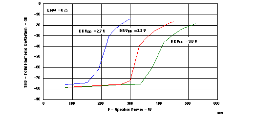
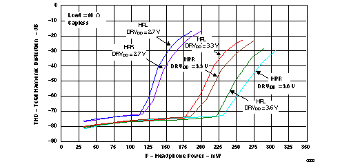
| Supply Voltage (AVDD, DRVDD) | 3.3 V |
| Supply Voltage (DVDD, IOVDD) | 1.8 V |
| Analog High-Power Output Driver load | 16 Ω |
| Analog Fully Differential Line Output Driver load | 10 kΩ |
12.2.1.2 Detailed Design Procedure
Using the Typical Application Schematic as a guide, integrate the hardware into the system.
Following the recommended component placement, schematic layout and routing given in the Layout Example section, integrate the device and its supporting components into the system PCB file.
- For questions and support go to the E2E forums (e2e.ti.com). If it is necessary to deviate from the recommended layout, visit the E2E forum to request a layout review.
Determining sample rate and Master clock frequency is required since powering up the device as all internal timing is derived from the master clock. Refer to the Figure 17 in order to get more information of how to configure correctly the required clocks for the device.
As the TLV320AIC3101 is designed for low-power applications, when powered up, the device has several features powered down. A correct routing of the TLV320AIC3101 signals is achieved by a correct setting of the device registers, powering up the required stages of the device and configuring the internal switches to follow a desired route.
For more information of the device configuration and programming, refer to the TLV320AIC3101 technical documents section in ti.com (http://www.ti.com/product/TLV320AIC3101/technicaldocuments).
12.2.1.3 Application Curves
12.2.2 Connections With Headphone and External Speaker Driver in Cell Phone Application
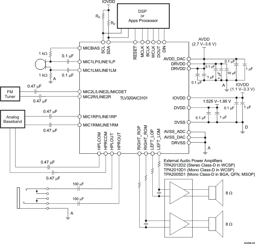 Figure 37. Typical Connections With Headphone and External Speaker Driver in Cell Phone Application
12.2.2.1 Design Requirements
See Analog Fully Differential Line Output Drivers section for the design requirements.
12.2.2.2 Detailed Design Procedure
See Analog Fully Differential Line Output Drivers section for the design requirements.
12.2.2.3 Application Curves
See Analog Fully Differential Line Output Drivers section for the application curves.